 |
Datenblatt-Suchmaschine für elektronische Bauteile |
|
|
Datenblatt-Suchmaschine für elektronische Bauteile |
|
The question interval is too short.
Please try again in a few seconds.

Hello, Please ask a question about MSM63V89C Datasheet
# Example questions:
➢ What is the maximum operating temperature specified in the datasheet for the msm63v89c?
➢ What must be done after the vcc reaches its specified voltage before using the device?
➢ What does the fam pin control and under what condition can it be set or released?
| Part No. | MSM63V89C |
| Manufacturer | OKI |
| Size | 141 Kbytes |
| Pages | 11 pages |
| Description | 1,048,576-Word x 1-Bit Solid-State Recorder Data Register |


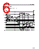



1. Product Overview:
️· Type: MOS Dynamic Read-Only Memory (DRAM). This is a DRAM chip, meaning it needs constant refreshing.
️· Capacity: 1024 x 16 = 16Kbit (though it's addressed as 1024 x 8 in some contexts)
️· Organization: Organized for byte-addressable access.
️· Intended Use: General-purpose electronic equipment for commercial applications. NOT intended for safety-critical applications (automotive, medical, aerospace, etc.).
2. Electrical & Performance Characteristics:
️· Supply Voltage (Vcc): Specification not explicitly mentioned here, but it's standard for DRAMs of this era.
️· Operating Temperature: Specification not explicitly mentioned, but typically -40°C to +85°C for commercial grade.
️· Refresh Requirements:
- Self-Refresh Mode: No external refresh control needed. This simplifies circuit design.
- Auto-Refresh Mode: Requires 1024 refresh cycles within 100ms.
️· Access Time: Specification not given directly but “Fast Access Mode” is available by keeping the FAM pin low.
️· Fast Access Mode (FAM): Provides faster read/write cycles if the FAM pin is held low, adhering to specific timing requirements (tFS and tSS - not detailed in the document). *Crucially, a normal cycle is needed afterward to increment the X address.*
3. Pin Functions (Key Ones):
️· A0-A9: Address lines (for selecting memory location).
️· D0-D7: Data input/output lines.
️· R/W: Read/Write control signal.
️· CS: Chip Select (enables/disables the chip).
️· RS/A: Self-Refresh/Auto-Refresh select. Determines refresh mode.
️· RFSH: Refresh Clock input (used in Auto-Refresh mode).
️· FAM: Fast Access Mode select.
️· TEST: Fixed high. Used internally during manufacturing.
️· D0-D7: Bi-directional data lines. High impedance when not selected (CS = High)
4. Key Operating Considerations & Special Features:
️· Power-Up Sequence: A critical detail. After applying power (Vcc), there is a 100ms stabilization period *before* normal operation. Followed by at least 8 RW cycles to initialize the memory.
️· Fast Access Mode (FAM): While offering improved speed, it requires careful implementation. It is dependent on specific timing.
️· Data Output: The output pins are in a high-impedance state when the chip is not selected. Allows for easy parallel connection of multiple MSM63V89C chips.
️· Memory Retention: Dependent on Vcc and temperature. (Specific retention times are not listed).
️· Package: TSOPII26/20-P-300-1.27-K. Surface mount. Requires care in handling and reflow soldering.
5. Important Notes & Warnings:
️· Non-Safety Critical: The device is specifically not approved for use in life-critical applications.
️· Export Restrictions: Possible government approval needed for export to certain countries.
️· Intellectual Property: No intellectual property rights granted for use.
️· Liability: Oki disclaims liability for misuse, improper handling, or failure to adhere to specifications.
️· Refresh Cycles: Must be performed in Auto Refresh mode within 100ms.
1. Product Overview:
️· Type: MOS Dynamic Read-Only Memory (DRAM). This is a DRAM chip, meaning it needs constant refreshing.
️· Capacity: 1024 x 16 = 16Kbit (though it's addressed as 1024 x 8 in some contexts)
️· Organization: Organized for byte-addressable access.
️· Intended Use: General-purpose electronic equipment for commercial applications. NOT intended for safety-critical applications (automotive, medical, aerospace, etc.).
2. Electrical & Performance Characteristics:
️· Supply Voltage (Vcc): Specification not explicitly mentioned here, but it's standard for DRAMs of this era.
️· Operating Temperature: Specification not explicitly mentioned, but typically -40°C to +85°C for commercial grade.
️· Refresh Requirements:
- Self-Refresh Mode: No external refresh control needed. This simplifies circuit design.
- Auto-Refresh Mode: Requires 1024 refresh cycles within 100ms.
️· Access Time: Specification not given directly but “Fast Access Mode” is available by keeping the FAM pin low.
️· Fast Access Mode (FAM): Provides faster read/write cycles if the FAM pin is held low, adhering to specific timing requirements (tFS and tSS - not detailed in the document). *Crucially, a normal cycle is needed afterward to increment the X address.*
3. Pin Functions (Key Ones):
️· A0-A9: Address lines (for selecting memory location).
️· D0-D7: Data input/output lines.
️· R/W: Read/Write control signal.
️· CS: Chip Select (enables/disables the chip).
️· RS/A: Self-Refresh/Auto-Refresh select. Determines refresh mode.
️· RFSH: Refresh Clock input (used in Auto-Refresh mode).
️· FAM: Fast Access Mode select.
️· TEST: Fixed high. Used internally during manufacturing.
️· D0-D7: Bi-directional data lines. High impedance when not selected (CS = High)
4. Key Operating Considerations & Special Features:
️· Power-Up Sequence: A critical detail. After applying power (Vcc), there is a 100ms stabilization period *before* normal operation. Followed by at least 8 RW cycles to initialize the memory.
️· Fast Access Mode (FAM): While offering improved speed, it requires careful implementation. It is dependent on specific timing.
️· Data Output: The output pins are in a high-impedance state when the chip is not selected. Allows for easy parallel connection of multiple MSM63V89C chips.
️· Memory Retention: Dependent on Vcc and temperature. (Specific retention times are not listed).
️· Package: TSOPII26/20-P-300-1.27-K. Surface mount. Requires care in handling and reflow soldering.
5. Important Notes & Warnings:
️· Non-Safety Critical: The device is specifically not approved for use in life-critical applications.
️· Export Restrictions: Possible government approval needed for export to certain countries.
️· Intellectual Property: No intellectual property rights granted for use.
️· Liability: Oki disclaims liability for misuse, improper handling, or failure to adhere to specifications.
️· Refresh Cycles: Must be performed in Auto Refresh mode within 100ms.
| Part No. | MSM63V89C |
| Manufacturer | OKI |
| Size | 141 Kbytes |
| Pages | 11 pages |
| Description | 1,048,576-Word x 1-Bit Solid-State Recorder Data Register |
| War ALLDATASHEET hilfreich? [ DONATE ] |
Über Alldatasheet | Werbung | Kontakt | Privatsphäre und Datenschutz | Link zum Datenblatt | Linktausch | Hersteller All Rights Reserved©Alldatasheet.com |
| Russian : Alldatasheetru.com | Korean : Alldatasheet.co.kr | Spanish : Alldatasheet.es | French : Alldatasheet.fr | Italian : Alldatasheetit.com Portuguese : Alldatasheetpt.com | Polish : Alldatasheet.pl | Vietnamese : Alldatasheet.vn Indian : Alldatasheet.in | Mexican : Alldatasheet.com.mx | British : Alldatasheet.co.uk | New Zealand : Alldatasheet.co.nz |
|
Family Site : ic2ic.com |
icmetro.com |
 German ▼
  English
 Chinese
 Japanese
 Russian
 Korean
 Spanish
 French
 Italian
 Portuguese
 Polish
 Vietnamese
 Indian
 Mexican
 British
 New Zealand