 |
Datenblatt-Suchmaschine für elektronische Bauteile |
|
|
Datenblatt-Suchmaschine für elektronische Bauteile |
|
The question interval is too short.
Please try again in a few seconds.

Hello, Please ask a question about HD74HC620 Datasheet
# Example questions:
➢ What is the approximate length of the 'd' dimension for the prsp0020dc-a package?
➢ What is the maximum supply voltage specified in the datasheet for the hd74hc620? (this information is not directly present but can be derived by reviewing the electrical characteristics section)
➢ What are the three package types listed in this datasheet with their corresponding renesas codes?
| Part No. | HD74HC620 |
| Manufacturer | RENESAS |
| Size | 128 Kbytes |
| Pages | 12 pages |
| Description | Octal Bus Transceivers (with inverted 3-state outputs),Octal Bus Transceivers (with 3-state outputs) |



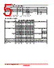

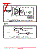


Document Type: Datasheet for the Renesas HD74HC620 and HD74HC623 Logic Gates.
Device Overview:
️· Function: These are high-speed CMOS logic gates – specifically, a quad 2-Input OR gate and a quad 2-Input NAND gate, respectively. (HD74HC620 is OR, HD74HC623 is NAND).
️· CMOS Technology: Built using advanced CMOS technology, providing low power consumption and high noise immunity.
️· Package Options: Available in several package types:
- DIP (Plastic Dual In-line Package)
- SOP (Small Outline Package) – multiple sizes and pitches (5.5x12.6-1.27 & 7.5x12.8-1.27)
Key Electrical Characteristics (Details are in the full datasheet, but generally):
️· Operating Voltage: Wide operating voltage range.
️· Input High Voltage (Vih): Typically around 2V
️· Output High Voltage (Voh): Dependent on Load and Vdd
️· Propagation Delay: Fast switching speeds
Important Features/Benefits:
️· High Speed: Designed for fast logic operations.
️· Low Power Consumption: CMOS technology minimizes power usage.
️· High Noise Immunity: Improved reliability in noisy environments.
️· Standard Logic Levels: Compatible with standard TTL and CMOS logic families.
️· Wide Operating Temperature: Suitable for a range of applications.
Document Contents:
️· Detailed Electrical Characteristics: (Voltage ranges, input/output current, propagation delays, etc.)
️· DC Characteristics: (Static performance of the gates)
️· AC Characteristics: (Switching speeds and dynamic performance)
️· Timing Diagrams: Illustrate the gate's behavior during switching transitions.
️· Package Dimensions: Detailed mechanical drawings of the various package options.
️· Sales and Support Contacts: Addresses and phone numbers for Renesas sales offices worldwide.
Where to Find More Information:
️· Renesas Website: [http://www.renesas.com](http://www.renesas.com)
️· Network Information: [http://www.renesas.com/en/network](http://www.renesas.com/en/network)
In essence, this document provides the technical specifications and information needed for engineers and designers to properly utilize the HD74HC620 and HD74HC623 logic gates in their electronic circuits.
Document Type: Datasheet for the Renesas HD74HC620 and HD74HC623 Logic Gates.
Device Overview:
️· Function: These are high-speed CMOS logic gates – specifically, a quad 2-Input OR gate and a quad 2-Input NAND gate, respectively. (HD74HC620 is OR, HD74HC623 is NAND).
️· CMOS Technology: Built using advanced CMOS technology, providing low power consumption and high noise immunity.
️· Package Options: Available in several package types:
- DIP (Plastic Dual In-line Package)
- SOP (Small Outline Package) – multiple sizes and pitches (5.5x12.6-1.27 & 7.5x12.8-1.27)
Key Electrical Characteristics (Details are in the full datasheet, but generally):
️· Operating Voltage: Wide operating voltage range.
️· Input High Voltage (Vih): Typically around 2V
️· Output High Voltage (Voh): Dependent on Load and Vdd
️· Propagation Delay: Fast switching speeds
Important Features/Benefits:
️· High Speed: Designed for fast logic operations.
️· Low Power Consumption: CMOS technology minimizes power usage.
️· High Noise Immunity: Improved reliability in noisy environments.
️· Standard Logic Levels: Compatible with standard TTL and CMOS logic families.
️· Wide Operating Temperature: Suitable for a range of applications.
Document Contents:
️· Detailed Electrical Characteristics: (Voltage ranges, input/output current, propagation delays, etc.)
️· DC Characteristics: (Static performance of the gates)
️· AC Characteristics: (Switching speeds and dynamic performance)
️· Timing Diagrams: Illustrate the gate's behavior during switching transitions.
️· Package Dimensions: Detailed mechanical drawings of the various package options.
️· Sales and Support Contacts: Addresses and phone numbers for Renesas sales offices worldwide.
Where to Find More Information:
️· Renesas Website: [http://www.renesas.com](http://www.renesas.com)
️· Network Information: [http://www.renesas.com/en/network](http://www.renesas.com/en/network)
In essence, this document provides the technical specifications and information needed for engineers and designers to properly utilize the HD74HC620 and HD74HC623 logic gates in their electronic circuits.
| Part No. | HD74HC620 |
| Manufacturer | RENESAS |
| Size | 128 Kbytes |
| Pages | 12 pages |
| Description | Octal Bus Transceivers (with inverted 3-state outputs),Octal Bus Transceivers (with 3-state outputs) |
| War ALLDATASHEET hilfreich? [ DONATE ] |
Über Alldatasheet | Werbung | Kontakt | Privatsphäre und Datenschutz | Link zum Datenblatt | Linktausch | Hersteller All Rights Reserved©Alldatasheet.com |
| Russian : Alldatasheetru.com | Korean : Alldatasheet.co.kr | Spanish : Alldatasheet.es | French : Alldatasheet.fr | Italian : Alldatasheetit.com Portuguese : Alldatasheetpt.com | Polish : Alldatasheet.pl | Vietnamese : Alldatasheet.vn Indian : Alldatasheet.in | Mexican : Alldatasheet.com.mx | British : Alldatasheet.co.uk | New Zealand : Alldatasheet.co.nz |
|
Family Site : ic2ic.com |
icmetro.com |
 German ▼
  English
 Chinese
 Japanese
 Russian
 Korean
 Spanish
 French
 Italian
 Portuguese
 Polish
 Vietnamese
 Indian
 Mexican
 British
 New Zealand