 |
Datenblatt-Suchmaschine für elektronische Bauteile |
|
|
Datenblatt-Suchmaschine für elektronische Bauteile |
|
The question interval is too short.
Please try again in a few seconds.

Hello, Please ask a question about SY10E151_08 Datasheet
# Example questions:
➢ In the provided truth table, what happens to the output qn(t+1) when the master reset (mr) input is high, regardless of the other inputs?
➢ If dn=h, clk1=u, clk2=l and mr=l, what is the value of qn(t+1)?
➢ What is the value of qn(t+1) when dn=l, clk1=u, clk2=l, and mr=h?
| Part No. | SY10E151_08 |
| Manufacturer | MICREL |
| Size | 64 Kbytes |
| Pages | 4 pages |
| Description | 6-BIT D REGISTER |


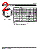

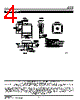

Understanding the Columns:
️· Dn: Data Input. This is the value being loaded into the flip-flop (or passed on).
️· CLK1, CLK2: Clock Inputs. These signals determine when the circuit changes state. The relationship between CLK1 and CLK2 is important and likely implements some form of clocking scheme.
️· MR (Mode Reset): A mode control signal. When activated, it often forces the output (Qn+1) to a specific state, overriding the input. This is a common way to control the initial state or reset the circuit.
️· Qn+1: The output of the circuit at the next clock cycle. It represents the resulting state after the data input and clock signals are evaluated. It is a function of Dn, CLK1, CLK2, and MR.
Analysis by Operation Mode:
Let's summarize the behavior based on different combinations of Clock and Mode signals. I'll broadly categorize into "Mode Reset (MR active)" and "Normal Operation (MR inactive)".
1. Mode Reset (MR = 1):
️· Regardless of the values of Dn, CLK1, and CLK2, the output Qn+1 is forced to '0'. This provides a way to initialize or reset the circuit to a known state.
2. Normal Operation (MR = 0):
This is where the interplay between CLK1, CLK2, and Dn determines the output. The behaviour of this behaviour is crucial for determining the kind of logic circuit it represents. Looking at the truth table, we can deduce some crucial observations:
️· Clock Relationship: Observe that the output change only occurs under certain combinations of CLK1 and CLK2. If a circuit requires both CLK1 and CLK2 to be high to trigger a change, it implies a certain type of latched behaviour and is not a simple edge triggered circuit.
️· Data input behavior: The change in Qn+1 is fully determined by the values of the clock signals (CLK1, CLK2) and the inputs Dn. There are cases where Qn+1 matches Dn.
What kind of Circuit is it?
Without more context, it’s difficult to say *exactly* what type of circuit this represents. It could be:
️· Clocked SR Flip-Flop Variant: The tables show an input Dn affecting the state of Qn+1. The mode reset functionality is common in flip-flops. The clocking signals being 2 separate clocks implies it is not a simple Edge triggered flip flop.
️· Latched Circuit: The behavior of Qn+1 based on the combination of clock signals suggests it could be a latched circuit with a more complex control scheme.
Understanding the Columns:
️· Dn: Data Input. This is the value being loaded into the flip-flop (or passed on).
️· CLK1, CLK2: Clock Inputs. These signals determine when the circuit changes state. The relationship between CLK1 and CLK2 is important and likely implements some form of clocking scheme.
️· MR (Mode Reset): A mode control signal. When activated, it often forces the output (Qn+1) to a specific state, overriding the input. This is a common way to control the initial state or reset the circuit.
️· Qn+1: The output of the circuit at the next clock cycle. It represents the resulting state after the data input and clock signals are evaluated. It is a function of Dn, CLK1, CLK2, and MR.
Analysis by Operation Mode:
Let's summarize the behavior based on different combinations of Clock and Mode signals. I'll broadly categorize into "Mode Reset (MR active)" and "Normal Operation (MR inactive)".
1. Mode Reset (MR = 1):
️· Regardless of the values of Dn, CLK1, and CLK2, the output Qn+1 is forced to '0'. This provides a way to initialize or reset the circuit to a known state.
2. Normal Operation (MR = 0):
This is where the interplay between CLK1, CLK2, and Dn determines the output. The behaviour of this behaviour is crucial for determining the kind of logic circuit it represents. Looking at the truth table, we can deduce some crucial observations:
️· Clock Relationship: Observe that the output change only occurs under certain combinations of CLK1 and CLK2. If a circuit requires both CLK1 and CLK2 to be high to trigger a change, it implies a certain type of latched behaviour and is not a simple edge triggered circuit.
️· Data input behavior: The change in Qn+1 is fully determined by the values of the clock signals (CLK1, CLK2) and the inputs Dn. There are cases where Qn+1 matches Dn.
What kind of Circuit is it?
Without more context, it’s difficult to say *exactly* what type of circuit this represents. It could be:
️· Clocked SR Flip-Flop Variant: The tables show an input Dn affecting the state of Qn+1. The mode reset functionality is common in flip-flops. The clocking signals being 2 separate clocks implies it is not a simple Edge triggered flip flop.
️· Latched Circuit: The behavior of Qn+1 based on the combination of clock signals suggests it could be a latched circuit with a more complex control scheme.
| Part No. | SY10E151_08 |
| Manufacturer | MICREL |
| Size | 64 Kbytes |
| Pages | 4 pages |
| Description | 6-BIT D REGISTER |
| War ALLDATASHEET hilfreich? [ DONATE ] |
Über Alldatasheet | Werbung | Kontakt | Privatsphäre und Datenschutz | Link zum Datenblatt | Linktausch | Hersteller All Rights Reserved©Alldatasheet.com |
| Russian : Alldatasheetru.com | Korean : Alldatasheet.co.kr | Spanish : Alldatasheet.es | French : Alldatasheet.fr | Italian : Alldatasheetit.com Portuguese : Alldatasheetpt.com | Polish : Alldatasheet.pl | Vietnamese : Alldatasheet.vn Indian : Alldatasheet.in | Mexican : Alldatasheet.com.mx | British : Alldatasheet.co.uk | New Zealand : Alldatasheet.co.nz |
|
Family Site : ic2ic.com |
icmetro.com |
 German ▼
  English
 Chinese
 Japanese
 Russian
 Korean
 Spanish
 French
 Italian
 Portuguese
 Polish
 Vietnamese
 Indian
 Mexican
 British
 New Zealand