 |
Datenblatt-Suchmaschine für elektronische Bauteile |
|
|
Datenblatt-Suchmaschine für elektronische Bauteile |
|
The question interval is too short.
Please try again in a few seconds.

Hello, Please ask a question about LT1358 Datasheet
# Example questions:
➢ What is the difference in power dissipation (pd) between cmos and lvds i/o modes at a 1msps sample rate during acquisition mode?
➢ What are the typical supply voltage ranges for vdd and vee, and what is the minimum required difference between them?
➢ How does the supply current (ivcc and ivee) change when switching between acquisition, nap, and power down modes at a 1msps sample rate?
| Part No. | LT1358 |
| Manufacturer | LINER |
| Size | 2Mb |
| Pages | 40 pages |
| Description | 18-Bit, 1Msps 8-Channel Differential 짹10.24V Input SoftSpan ADC with Wide Input Common Mode Range |


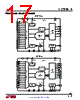


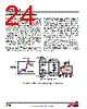


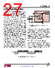


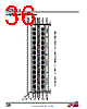


1. General Information (Implied):
️· Device: LTC2335-18 (High-Speed 18-bit ADC)
️· Sampling Rates: Capable of various sample rates (1Msps implied)
️· Grades: Different grades are available (C, H, I) affecting performance and power consumption.
️· Data Sheet Notes: Many values are defined at a specific temperature (25°C) and supply voltages unless otherwise noted. There are important Notes throughout the document related to specific measurements.
2. Power Requirements
This is a *massive* section, so I'm summarizing key values. The requirements depend heavily on the I/O mode (CMOS or LVDS) and grade (C, H, I).
️· Supply Voltages:
- VCC: 0 to 38V (Analog Supply)
- VEE: –16.5 to 0V (Analog Negative Supply)
- VDD: 4.75 to 5.25V (Digital Supply)
- OVDD (CMOS): 1.71 to 5.25V
- OVDD (LVDS): 2.375 to 5.25V
️· Supply Current (Approximate - Dependent on Mode & Grade): Ranges from a few microamps in power-down to 175-450mA at maximum performance. Power dissipation is a significant consideration. Refer to the table for specific current values depending on the mode and grade.
3. CMOS I/O Mode
️· Input Voltages:
- V<sub>IH</sub> (High Level Input): 0.8 x OVDD to OVDD
- V<sub>IL</sub> (Low Level Input): 0.2 x OVDD to 0
️· Output Voltages:
- V<sub>OH</sub> (High Level Output): OVDD – 0.2
- V<sub>OL</sub> (Low Level Output): 0.2
️· Power Dissipation (Example for H-Grade at 1Msps): ~204mW. This is just an example and changes with mode and grade.
4. LVDS I/O Mode
️· Differential Input Voltage (V<sub>ID</sub>): 200-600mV
️· On-Chip Input Termination Resistance (R<sub>ID</sub>): 90-125 Ω
️· Common Mode Input Voltage (V<sub>ICM</sub>): 0.3-2.2 V
️· Power Dissipation (Example for H-Grade at 1Msps): ~248mW. This is an example and varies with settings.
5. Key Highlights & Considerations
️· Grade Variations: The C, H, and I grades will have different performance characteristics (speed, noise) and, critically, different power consumption.
️· I/O Mode Impact: The choice of CMOS or LVDS I/O mode dramatically affects power consumption and signal integrity.
️· Power Management: The LTC2335-18 provides multiple power-down modes to minimize power consumption when not actively sampling. Proper use of these modes is critical for battery-powered applications.
️· Termination: The LVDS I/O mode requires careful termination to ensure proper signal integrity.
1. General Information (Implied):
️· Device: LTC2335-18 (High-Speed 18-bit ADC)
️· Sampling Rates: Capable of various sample rates (1Msps implied)
️· Grades: Different grades are available (C, H, I) affecting performance and power consumption.
️· Data Sheet Notes: Many values are defined at a specific temperature (25°C) and supply voltages unless otherwise noted. There are important Notes throughout the document related to specific measurements.
2. Power Requirements
This is a *massive* section, so I'm summarizing key values. The requirements depend heavily on the I/O mode (CMOS or LVDS) and grade (C, H, I).
️· Supply Voltages:
- VCC: 0 to 38V (Analog Supply)
- VEE: –16.5 to 0V (Analog Negative Supply)
- VDD: 4.75 to 5.25V (Digital Supply)
- OVDD (CMOS): 1.71 to 5.25V
- OVDD (LVDS): 2.375 to 5.25V
️· Supply Current (Approximate - Dependent on Mode & Grade): Ranges from a few microamps in power-down to 175-450mA at maximum performance. Power dissipation is a significant consideration. Refer to the table for specific current values depending on the mode and grade.
3. CMOS I/O Mode
️· Input Voltages:
- V<sub>IH</sub> (High Level Input): 0.8 x OVDD to OVDD
- V<sub>IL</sub> (Low Level Input): 0.2 x OVDD to 0
️· Output Voltages:
- V<sub>OH</sub> (High Level Output): OVDD – 0.2
- V<sub>OL</sub> (Low Level Output): 0.2
️· Power Dissipation (Example for H-Grade at 1Msps): ~204mW. This is just an example and changes with mode and grade.
4. LVDS I/O Mode
️· Differential Input Voltage (V<sub>ID</sub>): 200-600mV
️· On-Chip Input Termination Resistance (R<sub>ID</sub>): 90-125 Ω
️· Common Mode Input Voltage (V<sub>ICM</sub>): 0.3-2.2 V
️· Power Dissipation (Example for H-Grade at 1Msps): ~248mW. This is an example and varies with settings.
5. Key Highlights & Considerations
️· Grade Variations: The C, H, and I grades will have different performance characteristics (speed, noise) and, critically, different power consumption.
️· I/O Mode Impact: The choice of CMOS or LVDS I/O mode dramatically affects power consumption and signal integrity.
️· Power Management: The LTC2335-18 provides multiple power-down modes to minimize power consumption when not actively sampling. Proper use of these modes is critical for battery-powered applications.
️· Termination: The LVDS I/O mode requires careful termination to ensure proper signal integrity.
| Part No. | LT1358 |
| Manufacturer | LINER |
| Size | 2Mb |
| Pages | 40 pages |
| Description | 18-Bit, 1Msps 8-Channel Differential 짹10.24V Input SoftSpan ADC with Wide Input Common Mode Range |
| War ALLDATASHEET hilfreich? [ DONATE ] |
Über Alldatasheet | Werbung | Kontakt | Privatsphäre und Datenschutz | Link zum Datenblatt | Linktausch | Hersteller All Rights Reserved©Alldatasheet.com |
| Russian : Alldatasheetru.com | Korean : Alldatasheet.co.kr | Spanish : Alldatasheet.es | French : Alldatasheet.fr | Italian : Alldatasheetit.com Portuguese : Alldatasheetpt.com | Polish : Alldatasheet.pl | Vietnamese : Alldatasheet.vn Indian : Alldatasheet.in | Mexican : Alldatasheet.com.mx | British : Alldatasheet.co.uk | New Zealand : Alldatasheet.co.nz |
|
Family Site : ic2ic.com |
icmetro.com |
 German ▼
  English
 Chinese
 Japanese
 Russian
 Korean
 Spanish
 French
 Italian
 Portuguese
 Polish
 Vietnamese
 Indian
 Mexican
 British
 New Zealand