 |
Datenblatt-Suchmaschine für elektronische Bauteile |
|
|
Datenblatt-Suchmaschine für elektronische Bauteile |
|
The question interval is too short.
Please try again in a few seconds.

Hello, Please ask a question about H30PR5 Datasheet
# Example questions:
➢ What is the value of the non-repetitive peak collector current, as indicated in the maximum ratings table (though not explicitly stated, you'll need to scan the tables in the pdf).
➢ What major change was implemented in revision 2 compared to revision 1?
➢ What is the typical gate charge (qg) value for the ihw30n135r5 igbt, as shown in figure 17?
| Part No. | H30PR5 |
| Manufacturer | INFINEON |
| Size | 1Mb |
| Pages | 15 pages |
| Description | Reverse Conducting IGBT with monolithic body diode |






1. General Information & Revision History
️· Part Number: IHW30N135R5
️· Revision: 2.3 (as of September 20, 2019)
️· Document Type: IGBT Datasheet
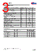
2. Key IGBT Electrical Characteristics (Based on available tables/figures. Note: A complete, organized table isn't provided across the entire document, so I'm extracting based on what's visible)
️· Voltage Blocking (V<sub>CES</sub>): 600 V (This is implied by various figures and the context)
️· Continuous Collector Current (I<sub>C</sub>): 30 A (Frequently used value in testing conditions)
️· Gate-Emitter Voltage (V<sub>GE</sub>): Varies during testing (see Figure C).
️· Input Capacitance (C<sub>ies</sub>): Value likely in the figures and tests.
️· Output Capacitance (C<sub>oss</sub>): Value likely in the figures and tests.
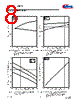
️· Gate Charge (Q<sub>g</sub>): See Figure 17 for values (around 16 nC at I<sub>C</sub> = 16 A).
️· Switching Times: This is detailed in testing circuits (Figure E)
- t<sub>on</sub>
- t<sub>off</sub>
- t<sub>rr</sub> (Reverse Recovery Time)
3. Diode Characteristics (Integrated within the IGBT)
️· Forward Voltage (V<sub>F</sub>): Ranges from 0 to 5V. Figure 21 provides a visual.
️· Forward Current (I<sub>F</sub>): Shown in relation to Forward Voltage (V<sub>F</sub>) in Figure 21
️· Junction Temperature (Tj): Affects V<sub>F</sub>
4. Thermal Characteristics
️· Thermal Resistance: Figures 19 and 20 show transient thermal resistance for IGBT and Diode.
️· Pulse Width: Associated with Thermal Resistance.
5. Testing Conditions and Circuits
️· Figure C: Defines diode switching characteristics.
️· Figure D: Not detailed in the provided data
️· Figure E: Dynamic test circuit – crucial for understanding the switching behavior. Includes parasitic inductance (L<sub>s</sub>), parasitic capacitance (C<sub>s</sub>), and a relief capacitor (C<sub>r</sub>, for ZVT switching).
️· Figure A & B: Illustrate testing setup and parameters.
6. Important Figures/Graphs & What They Show
️· Figure 21 (Typical Diode Forward Current vs. Forward Voltage): Shows the relationship between diode forward current and forward voltage. Crucial for understanding diode behavior.
️· Figure 17 (Typical Gate Charge): Illustrates the gate charge characteristics of the IGBT.
️· Figures 19 & 14 (Thermal Resistance & Losses): Shows relationship between thermal losses and junction temperature.
️· Figure 18 (Capacitance vs Collector-Emitter Voltage): Displays the capacitance as a function of collector-emitter voltage.
Key Takeaways & Notes:
️· Switching Performance: The dynamic test circuit (Figure E) and associated measurements (switching times, reverse recovery time) are critical for designing circuits that utilize this IGBT.
️· Thermal Management: Careful consideration of thermal resistance and power dissipation is essential.
️· ZVT Switching: The presence of a relief capacitor (C<sub>r</sub>) suggests this IGBT is designed to be compatible with ZVT (Zero Voltage Switching) techniques.
️· Datasheet Limitations: The provided data is a collection of figures and tables; a complete, organized datasheet table is not available. Some parameters may be hidden within the graphics.
1. General Information & Revision History
️· Part Number: IHW30N135R5
️· Revision: 2.3 (as of September 20, 2019)
️· Document Type: IGBT Datasheet
2. Key IGBT Electrical Characteristics (Based on available tables/figures. Note: A complete, organized table isn't provided across the entire document, so I'm extracting based on what's visible)
️· Voltage Blocking (V<sub>CES</sub>): 600 V (This is implied by various figures and the context)
️· Continuous Collector Current (I<sub>C</sub>): 30 A (Frequently used value in testing conditions)
️· Gate-Emitter Voltage (V<sub>GE</sub>): Varies during testing (see Figure C).
️· Input Capacitance (C<sub>ies</sub>): Value likely in the figures and tests.
️· Output Capacitance (C<sub>oss</sub>): Value likely in the figures and tests.
️· Gate Charge (Q<sub>g</sub>): See Figure 17 for values (around 16 nC at I<sub>C</sub> = 16 A).
️· Switching Times: This is detailed in testing circuits (Figure E)
- t<sub>on</sub>
- t<sub>off</sub>
- t<sub>rr</sub> (Reverse Recovery Time)
3. Diode Characteristics (Integrated within the IGBT)
️· Forward Voltage (V<sub>F</sub>): Ranges from 0 to 5V. Figure 21 provides a visual.
️· Forward Current (I<sub>F</sub>): Shown in relation to Forward Voltage (V<sub>F</sub>) in Figure 21
️· Junction Temperature (Tj): Affects V<sub>F</sub>
4. Thermal Characteristics
️· Thermal Resistance: Figures 19 and 20 show transient thermal resistance for IGBT and Diode.
️· Pulse Width: Associated with Thermal Resistance.
5. Testing Conditions and Circuits
️· Figure C: Defines diode switching characteristics.
️· Figure D: Not detailed in the provided data
️· Figure E: Dynamic test circuit – crucial for understanding the switching behavior. Includes parasitic inductance (L<sub>s</sub>), parasitic capacitance (C<sub>s</sub>), and a relief capacitor (C<sub>r</sub>, for ZVT switching).
️· Figure A & B: Illustrate testing setup and parameters.
6. Important Figures/Graphs & What They Show
️· Figure 21 (Typical Diode Forward Current vs. Forward Voltage): Shows the relationship between diode forward current and forward voltage. Crucial for understanding diode behavior.
️· Figure 17 (Typical Gate Charge): Illustrates the gate charge characteristics of the IGBT.
️· Figures 19 & 14 (Thermal Resistance & Losses): Shows relationship between thermal losses and junction temperature.
️· Figure 18 (Capacitance vs Collector-Emitter Voltage): Displays the capacitance as a function of collector-emitter voltage.
Key Takeaways & Notes:
️· Switching Performance: The dynamic test circuit (Figure E) and associated measurements (switching times, reverse recovery time) are critical for designing circuits that utilize this IGBT.
️· Thermal Management: Careful consideration of thermal resistance and power dissipation is essential.
️· ZVT Switching: The presence of a relief capacitor (C<sub>r</sub>) suggests this IGBT is designed to be compatible with ZVT (Zero Voltage Switching) techniques.
️· Datasheet Limitations: The provided data is a collection of figures and tables; a complete, organized datasheet table is not available. Some parameters may be hidden within the graphics.
| Part No. | H30PR5 |
| Manufacturer | INFINEON |
| Size | 1Mb |
| Pages | 15 pages |
| Description | Reverse Conducting IGBT with monolithic body diode |
| War ALLDATASHEET hilfreich? [ DONATE ] |
Über Alldatasheet | Werbung | Kontakt | Privatsphäre und Datenschutz | Link zum Datenblatt | Linktausch | Hersteller All Rights Reserved©Alldatasheet.com |
| Russian : Alldatasheetru.com | Korean : Alldatasheet.co.kr | Spanish : Alldatasheet.es | French : Alldatasheet.fr | Italian : Alldatasheetit.com Portuguese : Alldatasheetpt.com | Polish : Alldatasheet.pl | Vietnamese : Alldatasheet.vn Indian : Alldatasheet.in | Mexican : Alldatasheet.com.mx | British : Alldatasheet.co.uk | New Zealand : Alldatasheet.co.nz |
|
Family Site : ic2ic.com |
icmetro.com |
 German ▼
  English
 Chinese
 Japanese
 Russian
 Korean
 Spanish
 French
 Italian
 Portuguese
 Polish
 Vietnamese
 Indian
 Mexican
 British
 New Zealand