 |
Datenblatt-Suchmaschine für elektronische Bauteile |
|
|
Datenblatt-Suchmaschine für elektronische Bauteile |
|
The question interval is too short.
Please try again in a few seconds.

Hello, Please ask a question about V61C3181024 Datasheet
# Example questions:
➢ What must be kept in mind regarding the oe pin during a write cycle to avoid bus contention?
➢ What is the minimum write pulse width (twp) for the -10 speed grade of this sram?
➢ What is the difference between tcw1 and tcw2 as they relate to write cycle timing?
| Part No. | V61C3181024 |
| Manufacturer | MOSEL |
| Size | 77 Kbytes |
| Pages | 10 pages |
| Description | 128K X 8 HIGH SPEED STATIC RAM |





1. General Overview:
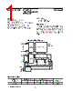
️· Type of Device: This is a memory chip, most likely SRAM (Static Random Access Memory).
️· Manufacturer: MOSEL
️· Part Number: V61C3181024 (appears frequently)
2. Key Specifications & Parameters (Extracted from Tables & Notes):
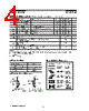
️· Operating Characteristics (Timing): The datasheet presents timing specifications (Read and Write Cycles) in a table format. It's important to notice the variation in timing parameters based on the speed grade (e.g., -10, -12, -15 ns).
- Read Cycle:
■ `tRC`: Read Cycle Time (e.g., 10, 12, 15 ns) - Minimum time required to complete a read operation.
■ `tAA`: Access Time - Time from input enabling to valid output data.
■ `tOE`: Output Enable Time
■ `tOLZ`: Output Low to High Z (Output Disable Time)
■ `tCHZ`: Chip Disable to Output High-Z
■ `tOHZ`: Output Disable to Output High-Z
■ `tOH`: Output Hold Time
- Write Cycle:
■ `tWC`: Write Cycle Time (e.g., 10, 12, 15 ns) – Minimum time required to complete a write operation.
■ `tCW`: Chip Enable to End of Write.
■ `tAW`: Address Valid to End of Write.
■ `tWP`: Write Pulse Width.
■ `tAH`: Address Hold Time.
■ `tDW`: Data Setup to End of Write.
■ `tDH`: Data Hold Time.
️· Voltages: (Not explicitly stated, but implied) - The chip likely operates on a standard voltage range (e.g., 3.3V or 5V), but this needs confirmation from another part of the full datasheet.
️· Input/Output Characteristics: (Limited detail, but hints at a standard CMOS interface).
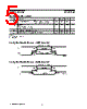
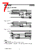
️· Switching Waveforms: Diagrams illustrate the timing relationships during Read and Write operations.
3. Important Notes & Clarifications:
️· CE (Chip Enable): The device uses CE1 and CE2 signals for controlling memory access.
️· WE (Write Enable): Used to initiate write operations.
️· OE (Output Enable): Used to drive the output. It is recommended to keep OE HIGH during write cycles.
️· Input/Output Conflicts: During a Write Cycle, the I/O pins can be in an output state, so input signals of the opposite phase must not be applied.
️· Timing Measurement Points: The document specifies that certain timing parameters are measured ±500mV from steady-state levels, with a specific load capacitance (C<sub>L</sub> = 5pF). This is crucial for accurate measurements.
️· Write Cycle Termination: The write cycle is terminated by the deactivation of any one of the control signals (CE1, CE2, WE).
4. Missing Information (What you'd need from a full datasheet):
️· Memory Capacity: The datasheet excerpt doesn't specify how much memory this chip holds (e.g., 1 Mbit, 2 Mbit).
️· Organization: Describes how the memory is arranged (e.g., number of banks, rows, columns).
️· Package Type: (e.g., DIP, SOIC, TSSOP).
️· Operating Temperature Range.
️· Power Consumption.
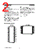
️· Pinout Diagram.
1. General Overview:
️· Type of Device: This is a memory chip, most likely SRAM (Static Random Access Memory).
️· Manufacturer: MOSEL
️· Part Number: V61C3181024 (appears frequently)
2. Key Specifications & Parameters (Extracted from Tables & Notes):
️· Operating Characteristics (Timing): The datasheet presents timing specifications (Read and Write Cycles) in a table format. It's important to notice the variation in timing parameters based on the speed grade (e.g., -10, -12, -15 ns).
- Read Cycle:
■ `tRC`: Read Cycle Time (e.g., 10, 12, 15 ns) - Minimum time required to complete a read operation.
■ `tAA`: Access Time - Time from input enabling to valid output data.
■ `tOE`: Output Enable Time
■ `tOLZ`: Output Low to High Z (Output Disable Time)
■ `tCHZ`: Chip Disable to Output High-Z
■ `tOHZ`: Output Disable to Output High-Z
■ `tOH`: Output Hold Time
- Write Cycle:
■ `tWC`: Write Cycle Time (e.g., 10, 12, 15 ns) – Minimum time required to complete a write operation.
■ `tCW`: Chip Enable to End of Write.
■ `tAW`: Address Valid to End of Write.
■ `tWP`: Write Pulse Width.
■ `tAH`: Address Hold Time.
■ `tDW`: Data Setup to End of Write.
■ `tDH`: Data Hold Time.
️· Voltages: (Not explicitly stated, but implied) - The chip likely operates on a standard voltage range (e.g., 3.3V or 5V), but this needs confirmation from another part of the full datasheet.
️· Input/Output Characteristics: (Limited detail, but hints at a standard CMOS interface).
️· Switching Waveforms: Diagrams illustrate the timing relationships during Read and Write operations.
3. Important Notes & Clarifications:
️· CE (Chip Enable): The device uses CE1 and CE2 signals for controlling memory access.
️· WE (Write Enable): Used to initiate write operations.
️· OE (Output Enable): Used to drive the output. It is recommended to keep OE HIGH during write cycles.
️· Input/Output Conflicts: During a Write Cycle, the I/O pins can be in an output state, so input signals of the opposite phase must not be applied.
️· Timing Measurement Points: The document specifies that certain timing parameters are measured ±500mV from steady-state levels, with a specific load capacitance (C<sub>L</sub> = 5pF). This is crucial for accurate measurements.
️· Write Cycle Termination: The write cycle is terminated by the deactivation of any one of the control signals (CE1, CE2, WE).
4. Missing Information (What you'd need from a full datasheet):
️· Memory Capacity: The datasheet excerpt doesn't specify how much memory this chip holds (e.g., 1 Mbit, 2 Mbit).
️· Organization: Describes how the memory is arranged (e.g., number of banks, rows, columns).
️· Package Type: (e.g., DIP, SOIC, TSSOP).
️· Operating Temperature Range.
️· Power Consumption.
️· Pinout Diagram.
| Part No. | V61C3181024 |
| Manufacturer | MOSEL |
| Size | 77 Kbytes |
| Pages | 10 pages |
| Description | 128K X 8 HIGH SPEED STATIC RAM |
| War ALLDATASHEET hilfreich? [ DONATE ] |
Über Alldatasheet | Werbung | Kontakt | Privatsphäre und Datenschutz | Link zum Datenblatt | Linktausch | Hersteller All Rights Reserved©Alldatasheet.com |
| Russian : Alldatasheetru.com | Korean : Alldatasheet.co.kr | Spanish : Alldatasheet.es | French : Alldatasheet.fr | Italian : Alldatasheetit.com Portuguese : Alldatasheetpt.com | Polish : Alldatasheet.pl | Vietnamese : Alldatasheet.vn Indian : Alldatasheet.in | Mexican : Alldatasheet.com.mx | British : Alldatasheet.co.uk | New Zealand : Alldatasheet.co.nz |
|
Family Site : ic2ic.com |
icmetro.com |
 German ▼
  English
 Chinese
 Japanese
 Russian
 Korean
 Spanish
 French
 Italian
 Portuguese
 Polish
 Vietnamese
 Indian
 Mexican
 British
 New Zealand