 |
Datenblatt-Suchmaschine für elektronische Bauteile |
|
|
Datenblatt-Suchmaschine für elektronische Bauteile |
|
The question interval is too short.
Please try again in a few seconds.

Hello, Please ask a question about V61C51161024 Datasheet
# Example questions:
➢ What is the minimum write pulse width (twp) for the -10 speed grade?
➢ Referring to the 'read cycle 1' waveform, what signals must be asserted to initiate a read operation, and what is the role of the oe (output enable) signal during this cycle?
➢ What are the two package types available for this memory chip?
| Part No. | V61C51161024 |
| Manufacturer | MOSEL |
| Size | 61 Kbytes |
| Pages | 10 pages |
| Description | 64K x 16 HIGH SPEED STATIC RAM |





1. Basic Information:
️· Part Number: V61C51161024
️· Type: DRAM (Dynamic Random Access Memory)
️· Capacity: 512K x 2 (1 Megabit)
️· Organization: 512K x 2
️· Manufacturer: MOS Electric
2. Features:
️· Standard DRAM interface
️· Available in a 44-pin TSOP-II package (Thin Small Outline Package)
️· Standard Operating Voltage: Unspecified (likely 3.3V or 5V - need further confirmation)
️· Timing Specifications are dependent on the specific temperature range (-40°C to +85°C).
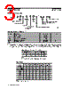
3. Key Electrical Characteristics:
️· This is a comprehensive datasheet, so many electrical parameters are detailed. Some key points:
- Write Cycle Time: Around 10-15 ns (varies with temperature)
- Read Cycle Time: Around 10-15 ns (varies with temperature)
- Address Setup and Hold Times: Critical for reliable operation, specific values are provided based on temperature.
- Power Supply Requirements: The datasheet doesn't explicitly state the voltage, but the data would indicate a standard voltage.
- Input and Output Characteristics: Details about drive strength, load capacities, and voltage levels.
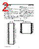
4. Pinout and Package:
️· Package Type: 44-pin TSOP-II
️· The datasheet provides a diagram of the package with pin numbers and key dimensions.
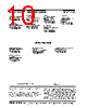
5. Operating Modes/Timing Diagrams:
️· The datasheet includes diagrams showing the timing for:
- Read Cycles (including variations in how the cycle is controlled)
- Write Cycles (controlled by WE and CE signals)
️· Important signals include:
- CE (Chip Enable)
- WE (Write Enable)
- OE (Output Enable)
- UBE, LBE (Upper/Lower Byte Enable)
- RAS (Row Address Strobe)
- CAS (Column Address Strobe)
6. Important Notes:
️· Temperature Dependence: All timing specifications are heavily influenced by operating temperature.
️· Signal Integrity: Careful attention to signal integrity is crucial for reliable operation. Proper termination and decoupling are recommended.
️· Bus Contention: It's recommended to keep OE high during write cycles to avoid bus contention.
To fully understand and implement this DRAM, you would need to:
️· Confirm the operating voltage: This is not explicitly stated in this extract.
️· Refer to the full datasheet: This summary is based on a partial extract. A complete datasheet would provide much more detail.
️· Carefully analyze the timing diagrams to ensure correct sequencing and timing of signals.
1. Basic Information:
️· Part Number: V61C51161024
️· Type: DRAM (Dynamic Random Access Memory)
️· Capacity: 512K x 2 (1 Megabit)
️· Organization: 512K x 2
️· Manufacturer: MOS Electric
2. Features:
️· Standard DRAM interface
️· Available in a 44-pin TSOP-II package (Thin Small Outline Package)
️· Standard Operating Voltage: Unspecified (likely 3.3V or 5V - need further confirmation)
️· Timing Specifications are dependent on the specific temperature range (-40°C to +85°C).
3. Key Electrical Characteristics:
️· This is a comprehensive datasheet, so many electrical parameters are detailed. Some key points:
- Write Cycle Time: Around 10-15 ns (varies with temperature)
- Read Cycle Time: Around 10-15 ns (varies with temperature)
- Address Setup and Hold Times: Critical for reliable operation, specific values are provided based on temperature.
- Power Supply Requirements: The datasheet doesn't explicitly state the voltage, but the data would indicate a standard voltage.
- Input and Output Characteristics: Details about drive strength, load capacities, and voltage levels.
4. Pinout and Package:
️· Package Type: 44-pin TSOP-II
️· The datasheet provides a diagram of the package with pin numbers and key dimensions.
5. Operating Modes/Timing Diagrams:
️· The datasheet includes diagrams showing the timing for:
- Read Cycles (including variations in how the cycle is controlled)
- Write Cycles (controlled by WE and CE signals)
️· Important signals include:
- CE (Chip Enable)
- WE (Write Enable)
- OE (Output Enable)
- UBE, LBE (Upper/Lower Byte Enable)
- RAS (Row Address Strobe)
- CAS (Column Address Strobe)
6. Important Notes:
️· Temperature Dependence: All timing specifications are heavily influenced by operating temperature.
️· Signal Integrity: Careful attention to signal integrity is crucial for reliable operation. Proper termination and decoupling are recommended.
️· Bus Contention: It's recommended to keep OE high during write cycles to avoid bus contention.
To fully understand and implement this DRAM, you would need to:
️· Confirm the operating voltage: This is not explicitly stated in this extract.
️· Refer to the full datasheet: This summary is based on a partial extract. A complete datasheet would provide much more detail.
️· Carefully analyze the timing diagrams to ensure correct sequencing and timing of signals.
| Part No. | V61C51161024 |
| Manufacturer | MOSEL |
| Size | 61 Kbytes |
| Pages | 10 pages |
| Description | 64K x 16 HIGH SPEED STATIC RAM |
| War ALLDATASHEET hilfreich? [ DONATE ] |
Über Alldatasheet | Werbung | Kontakt | Privatsphäre und Datenschutz | Link zum Datenblatt | Linktausch | Hersteller All Rights Reserved©Alldatasheet.com |
| Russian : Alldatasheetru.com | Korean : Alldatasheet.co.kr | Spanish : Alldatasheet.es | French : Alldatasheet.fr | Italian : Alldatasheetit.com Portuguese : Alldatasheetpt.com | Polish : Alldatasheet.pl | Vietnamese : Alldatasheet.vn Indian : Alldatasheet.in | Mexican : Alldatasheet.com.mx | British : Alldatasheet.co.uk | New Zealand : Alldatasheet.co.nz |
|
Family Site : ic2ic.com |
icmetro.com |
 German ▼
  English
 Chinese
 Japanese
 Russian
 Korean
 Spanish
 French
 Italian
 Portuguese
 Polish
 Vietnamese
 Indian
 Mexican
 British
 New Zealand