 |
Datenblatt-Suchmaschine für elektronische Bauteile |
|
|
Datenblatt-Suchmaschine für elektronische Bauteile |
|
The question interval is too short.
Please try again in a few seconds.

Hello, Please ask a question about ML74WLCF Datasheet
# Example questions:
➢ What is the typical quiescent supply current (icc) when vcc is 5.5v?
➢ What is the value of input capacitance (cin) specified in the switching electrical characteristics table?
➢ What is the maximum storage temperature specified for this device?
| Part No. | ML74WLCF |
| Manufacturer | MINILOGIC |
| Size | 145 Kbytes |
| Pages | 4 pages |
| Description | Inverter (unbuffered) and Buffer |

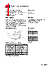
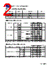
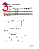
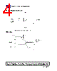

1. Product Identification and Overview
️· Type: Logic Gate (likely an inverter or buffer, based on the description).
️· Function: Provides both standard (high to high) and inverted (high to low) logic functions.
️· Revision: Rev. B, September 2005
2. Features & Functionality
️· Inverter/Buffer Functionality: Can either pass a signal unchanged (buffer) or invert it.
️· Logic Levels: Operates with both High and Low logic levels.
3. Absolute Maximum Ratings (Stress Limits)
These are the extreme conditions the chip can handle without permanent damage. *Exceeding these can destroy the device.*
️· Supply Voltage (Vcc): -0.5V to +6.0V
️· Input Voltage (Vin): -0.5V to +6.0V
️· Output Voltage (Vout): -0.5V to Vcc + 0.5V
️· Input Diode Current (Iik): ±20mA
️· Output Diode Current (Iok): ±20mA
️· Switch Output Current (Iout): ±25mA
️· Power Dissipation (Pd): 300mW
️· Storage Temperature: -65°C to +150°C
4. Recommended Operating Conditions
These are the *typical* conditions for reliable operation.
️· Supply Voltage (Vcc): 2V to 5.5V
️· Input Voltage: 0V to 5.5V
️· Output Voltage: 0V to Vcc
️· Operating Temperature: -40°C to +85°C
️· Input Rise/Fall Time: Varies based on supply voltage (specific values given)
5. DC Electrical Characteristics
This is the heart of the datasheet, providing specific voltage levels for different logic states. Includes:
️· Input High Voltage (Vih): Voltage required for a logic "1" at the input.
️· Input Low Voltage (Vil): Voltage that is recognized as a logic "0" at the input.
️· Output High Voltage (Voh): Voltage at the output when the input is a logic "1".
️· Output Low Voltage (Vol): Voltage at the output when the input is a logic "0".
️· Input Current (Iin): Current drawn by the input pins.
️· Quiescent Supply Current (Icc): Supply current when the output is not driving a load.
6. Switching Electrical Characteristics
Defines how quickly the chip can change states.
️· Propagation Delay Time (tPLH & tPHL): Time it takes for the output to respond to a change at the input. These are crucial for timing critical applications.
️· Input Capacitance (Cin): A measure of how much charge needs to be supplied to the input.
️· Power Dissipation Capacitance (Cpd): The capacitance associated with power dissipation.
7. Noise Characteristics
Specifies the noise immunity of the chip.
️· Dynamic VOL and VOH: Maximum and minimum output voltage under noisy conditions.
️· VIHD, VILD: The voltage at the inputs to maintain stable operation.
8. Application Information
️· A typical application circuit diagram.
️· A note about how to measure supply current.
9. Disclaimer:
Standard legal statement limiting liability.
Key Takeaways
️· This is a foundational logic gate (likely an inverter or buffer) designed for digital circuit applications.
️· It's a relatively older part (2005) – newer parts will have improved characteristics.
️· The datasheet is filled with numbers and technical terms important for engineers designing digital circuits.
️· Understanding these specifications allows engineers to make informed decisions about whether this chip is suitable for their application.
1. Product Identification and Overview
️· Type: Logic Gate (likely an inverter or buffer, based on the description).
️· Function: Provides both standard (high to high) and inverted (high to low) logic functions.
️· Revision: Rev. B, September 2005
2. Features & Functionality
️· Inverter/Buffer Functionality: Can either pass a signal unchanged (buffer) or invert it.
️· Logic Levels: Operates with both High and Low logic levels.
3. Absolute Maximum Ratings (Stress Limits)
These are the extreme conditions the chip can handle without permanent damage. *Exceeding these can destroy the device.*
️· Supply Voltage (Vcc): -0.5V to +6.0V
️· Input Voltage (Vin): -0.5V to +6.0V
️· Output Voltage (Vout): -0.5V to Vcc + 0.5V
️· Input Diode Current (Iik): ±20mA
️· Output Diode Current (Iok): ±20mA
️· Switch Output Current (Iout): ±25mA
️· Power Dissipation (Pd): 300mW
️· Storage Temperature: -65°C to +150°C
4. Recommended Operating Conditions
These are the *typical* conditions for reliable operation.
️· Supply Voltage (Vcc): 2V to 5.5V
️· Input Voltage: 0V to 5.5V
️· Output Voltage: 0V to Vcc
️· Operating Temperature: -40°C to +85°C
️· Input Rise/Fall Time: Varies based on supply voltage (specific values given)
5. DC Electrical Characteristics
This is the heart of the datasheet, providing specific voltage levels for different logic states. Includes:
️· Input High Voltage (Vih): Voltage required for a logic "1" at the input.
️· Input Low Voltage (Vil): Voltage that is recognized as a logic "0" at the input.
️· Output High Voltage (Voh): Voltage at the output when the input is a logic "1".
️· Output Low Voltage (Vol): Voltage at the output when the input is a logic "0".
️· Input Current (Iin): Current drawn by the input pins.
️· Quiescent Supply Current (Icc): Supply current when the output is not driving a load.
6. Switching Electrical Characteristics
Defines how quickly the chip can change states.
️· Propagation Delay Time (tPLH & tPHL): Time it takes for the output to respond to a change at the input. These are crucial for timing critical applications.
️· Input Capacitance (Cin): A measure of how much charge needs to be supplied to the input.
️· Power Dissipation Capacitance (Cpd): The capacitance associated with power dissipation.
7. Noise Characteristics
Specifies the noise immunity of the chip.
️· Dynamic VOL and VOH: Maximum and minimum output voltage under noisy conditions.
️· VIHD, VILD: The voltage at the inputs to maintain stable operation.
8. Application Information
️· A typical application circuit diagram.
️· A note about how to measure supply current.
9. Disclaimer:
Standard legal statement limiting liability.
Key Takeaways
️· This is a foundational logic gate (likely an inverter or buffer) designed for digital circuit applications.
️· It's a relatively older part (2005) – newer parts will have improved characteristics.
️· The datasheet is filled with numbers and technical terms important for engineers designing digital circuits.
️· Understanding these specifications allows engineers to make informed decisions about whether this chip is suitable for their application.
| Part No. | ML74WLCF |
| Manufacturer | MINILOGIC |
| Size | 145 Kbytes |
| Pages | 4 pages |
| Description | Inverter (unbuffered) and Buffer |
| War ALLDATASHEET hilfreich? [ DONATE ] |
Über Alldatasheet | Werbung | Kontakt | Privatsphäre und Datenschutz | Link zum Datenblatt | Linktausch | Hersteller All Rights Reserved©Alldatasheet.com |
| Russian : Alldatasheetru.com | Korean : Alldatasheet.co.kr | Spanish : Alldatasheet.es | French : Alldatasheet.fr | Italian : Alldatasheetit.com Portuguese : Alldatasheetpt.com | Polish : Alldatasheet.pl | Vietnamese : Alldatasheet.vn Indian : Alldatasheet.in | Mexican : Alldatasheet.com.mx | British : Alldatasheet.co.uk | New Zealand : Alldatasheet.co.nz |
|
Family Site : ic2ic.com |
icmetro.com |
 German ▼
  English
 Chinese
 Japanese
 Russian
 Korean
 Spanish
 French
 Italian
 Portuguese
 Polish
 Vietnamese
 Indian
 Mexican
 British
 New Zealand