 |
Datenblatt-Suchmaschine für elektronische Bauteile |
|
|
Datenblatt-Suchmaschine für elektronische Bauteile |
|
The question interval is too short.
Please try again in a few seconds.

Hello, Please ask a question about IXFN30N120P Datasheet
# Example questions:
➢ What happens to capacitance (ciss, coss, crss) as the drain-source voltage (vds) increases, assuming a fixed frequency of 1 mhz?
➢ Examine figure 1, and explain how the pulse width affects the current capability of the device. what is the approximate current limit at a pulse width of 1 second?
➢ How does increasing the junction temperature (tj) generally affect the forward voltage drop of the intrinsic diode?
| Part No. | IXFN30N120P |
| Manufacturer | IXYS |
| Size | 114 Kbytes |
| Pages | 4 pages |
| Description | Polar Power MOSFET HiPerFET |


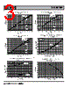


1. General Information & Key Parameters (Inferred - not directly labeled)
️· Device Type: N-Channel MOSFET (likely a Power MOSFET)
️· Voltage Rating (Vds): 120V (judging from the name)
️· Current Rating (Id): Likely a fairly high current device, though the exact value isn't explicitly stated on the image.
️· Manufacturer: IXYS
️· Part Number: Likely 30N120P (based on figure reference)
2. Figures & Data - Detailed Breakdown
I'll describe each figure roughly in order of appearance and significance. I'm providing some assumptions based on common data sheet conventions.
️· Figure 1: Forward Voltage Drop of Intrinsic Diode (9)
- Shows the voltage across the body diode (intrinsic diode) as a function of current. Typical characteristic of a power MOSFET. Forward voltage increases with increasing current.
️· Figure 2: Drain-Source Voltage vs. Gate-Source Voltage (Threshold Voltage) (10)
- Shows the drain-source voltage as a function of gate-source voltage. This defines the threshold voltage (Vgs(th)) which is the minimum gate-source voltage required to turn the MOSFET on.
️· Figure 3: Static Drain-Source Characteristics (11)
- Plots drain current (Id) vs. drain-source voltage (Vds) at various gate-source voltage (Vgs) values. Shows how the device's current handling changes with applied voltage and gate drive.
️· Figure 4: Forward Voltage Drop of Intrinsic Diode (9)
- Similar to Figure 1, but with data.
️· Figure 11: Capacitance
- Plots capacitance (Ciss, Coss, Crss) versus Drain-Source Voltage (Vds) at a specific Gate-Source Voltage (Vgs). These values are important for high-frequency circuit design.
️· Figure 7: Input Capacitance
- Similar to Figure 11, providing specific capacitance values.
️· Figure 12: Safe Operating Area
- This is a crucial figure. It shows the maximum drain current (Id) vs. drain-source voltage (Vds) that the device can handle without exceeding its maximum power dissipation. The allowable region is the area *below* the curve. Exceeding this can cause permanent damage. This figure likely includes various thermal conditions.
️· Figure 5: Characteristics (Implied from numbering)
- Drain-Source Leakage Current vs. Voltage
️· Figure 6: Switching Time
- Shows how quickly the MOSFET switches between "on" and "off" states. Important for high-frequency power conversion applications. Includes rise and fall times.
️· Figure 5: Characteristics (Implied from numbering)
- Drain-Source Leakage Current vs. Voltage
️· Figure 8: Characteristics (Implied from numbering)
- A graph detailing device switching parameters (Rise and Fall Times)
️· Figure 10: Transient Thermal Impedance
- Shows how the temperature of the device increases over time when it's dissipating power. This is crucial for thermal management.
️· Figure 9: Safe Operating Area
- The area where the device can safely operate at a certain power dissipation.
️· Figure 4: Characteristics
- Shows the MOSFET output voltage versus time.
️· Figure 5: Characteristics
- Shows MOSFET voltage versus time.
Difficulties & Assumptions
️· Labeling and Resolution: Some of the axes and labels are difficult to read due to the image quality. I’m making educated guesses.
️· Context: Without the full data sheet, some of the figures may have specific nuances I can’t fully interpret.
️· Units: While I’m providing general units (Volts, Amps, Seconds), some figures might use different prefixes (e.g., nS for nanoseconds).
Overall Summary:
The data sheet describes a 120V power MOSFET with relatively high current handling capability. It provides essential information for designing circuits that use this MOSFET, including its electrical characteristics, switching performance, safe operating area, and thermal behavior. Understanding these parameters is vital for ensuring reliable operation and preventing damage to the device.
1. General Information & Key Parameters (Inferred - not directly labeled)
️· Device Type: N-Channel MOSFET (likely a Power MOSFET)
️· Voltage Rating (Vds): 120V (judging from the name)
️· Current Rating (Id): Likely a fairly high current device, though the exact value isn't explicitly stated on the image.
️· Manufacturer: IXYS
️· Part Number: Likely 30N120P (based on figure reference)
2. Figures & Data - Detailed Breakdown
I'll describe each figure roughly in order of appearance and significance. I'm providing some assumptions based on common data sheet conventions.
️· Figure 1: Forward Voltage Drop of Intrinsic Diode (9)
- Shows the voltage across the body diode (intrinsic diode) as a function of current. Typical characteristic of a power MOSFET. Forward voltage increases with increasing current.
️· Figure 2: Drain-Source Voltage vs. Gate-Source Voltage (Threshold Voltage) (10)
- Shows the drain-source voltage as a function of gate-source voltage. This defines the threshold voltage (Vgs(th)) which is the minimum gate-source voltage required to turn the MOSFET on.
️· Figure 3: Static Drain-Source Characteristics (11)
- Plots drain current (Id) vs. drain-source voltage (Vds) at various gate-source voltage (Vgs) values. Shows how the device's current handling changes with applied voltage and gate drive.
️· Figure 4: Forward Voltage Drop of Intrinsic Diode (9)
- Similar to Figure 1, but with data.
️· Figure 11: Capacitance
- Plots capacitance (Ciss, Coss, Crss) versus Drain-Source Voltage (Vds) at a specific Gate-Source Voltage (Vgs). These values are important for high-frequency circuit design.
️· Figure 7: Input Capacitance
- Similar to Figure 11, providing specific capacitance values.
️· Figure 12: Safe Operating Area
- This is a crucial figure. It shows the maximum drain current (Id) vs. drain-source voltage (Vds) that the device can handle without exceeding its maximum power dissipation. The allowable region is the area *below* the curve. Exceeding this can cause permanent damage. This figure likely includes various thermal conditions.
️· Figure 5: Characteristics (Implied from numbering)
- Drain-Source Leakage Current vs. Voltage
️· Figure 6: Switching Time
- Shows how quickly the MOSFET switches between "on" and "off" states. Important for high-frequency power conversion applications. Includes rise and fall times.
️· Figure 5: Characteristics (Implied from numbering)
- Drain-Source Leakage Current vs. Voltage
️· Figure 8: Characteristics (Implied from numbering)
- A graph detailing device switching parameters (Rise and Fall Times)
️· Figure 10: Transient Thermal Impedance
- Shows how the temperature of the device increases over time when it's dissipating power. This is crucial for thermal management.
️· Figure 9: Safe Operating Area
- The area where the device can safely operate at a certain power dissipation.
️· Figure 4: Characteristics
- Shows the MOSFET output voltage versus time.
️· Figure 5: Characteristics
- Shows MOSFET voltage versus time.
Difficulties & Assumptions
️· Labeling and Resolution: Some of the axes and labels are difficult to read due to the image quality. I’m making educated guesses.
️· Context: Without the full data sheet, some of the figures may have specific nuances I can’t fully interpret.
️· Units: While I’m providing general units (Volts, Amps, Seconds), some figures might use different prefixes (e.g., nS for nanoseconds).
Overall Summary:
The data sheet describes a 120V power MOSFET with relatively high current handling capability. It provides essential information for designing circuits that use this MOSFET, including its electrical characteristics, switching performance, safe operating area, and thermal behavior. Understanding these parameters is vital for ensuring reliable operation and preventing damage to the device.
| Part No. | IXFN30N120P |
| Manufacturer | IXYS |
| Size | 114 Kbytes |
| Pages | 4 pages |
| Description | Polar Power MOSFET HiPerFET |
| War ALLDATASHEET hilfreich? [ DONATE ] |
Über Alldatasheet | Werbung | Kontakt | Privatsphäre und Datenschutz | Link zum Datenblatt | Linktausch | Hersteller All Rights Reserved©Alldatasheet.com |
| Russian : Alldatasheetru.com | Korean : Alldatasheet.co.kr | Spanish : Alldatasheet.es | French : Alldatasheet.fr | Italian : Alldatasheetit.com Portuguese : Alldatasheetpt.com | Polish : Alldatasheet.pl | Vietnamese : Alldatasheet.vn Indian : Alldatasheet.in | Mexican : Alldatasheet.com.mx | British : Alldatasheet.co.uk | New Zealand : Alldatasheet.co.nz |
|
Family Site : ic2ic.com |
icmetro.com |
 German ▼
  English
 Chinese
 Japanese
 Russian
 Korean
 Spanish
 French
 Italian
 Portuguese
 Polish
 Vietnamese
 Indian
 Mexican
 British
 New Zealand