 |
Datenblatt-Suchmaschine für elektronische Bauteile |
|
|
Datenblatt-Suchmaschine für elektronische Bauteile |
|
The question interval is too short.
Please try again in a few seconds.

Hello, Please ask a question about SN54LS398 Datasheet
# Example questions:
➢ What is the maximum output low voltage (vol) for the 74ls series when the output current (iol) is 8.0ma?
➢ What are the key differences in operating temperature ranges between the 54 and 74 series devices described in the document?
➢ What is the minimum data setup time (ts) required for predictable output performance?
| Part No. | SN54LS398 |
| Manufacturer | MOTOROLA |
| Size | 209 Kbytes |
| Pages | 6 pages |
| Description | QUAD 2-PORT REGISTER |

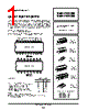




1. Device Overview:
️· Part Number: 74LS398 (multiple suffixes exist like 'D', 'J', 'N' influencing package type)
️· Type: 8-bit Data Register with 3-State Outputs
️· Function: This is a shift register. Data is shifted in serially and appears in parallel at the outputs. The 3-state outputs allow the register to be easily connected in series to create long shift register chains. It essentially takes a serial bit stream and converts it into a parallel byte.
️· Key Features:
- Serial data input
- Parallel data output
- 3-state outputs (active high, enabled by a control signal)
- Allows cascading for extended data shifting
- Standard LS TTL compatibility
2. Key Specifications (DC Characteristics):
️· Supply Voltage (VCC):
- 74LS398: 5.0V to 5.5V
- 74LS398D: 4.5V to 5.5V
️· Input HIGH Voltage (VIH):
- 74LS398: 2.0V
- 74LS398D: 2.0V
️· Input LOW Voltage (VIL):
- 74LS398: 0.8V
- 74LS398D: 0.8V
️· Output HIGH Voltage (VOH):
- VCC = 5.0V, IOH = -4.0mA (74LS398) / -8.0mA (74LS398D)
️· Output LOW Voltage (VOL):
- IOL = 8.0mA (74LS398D) / 4.0mA (74LS398)
️· Input Current (IIH & IIL): Specifies the current drawn into the inputs.
️· Power Supply Current (ICC): A typical value of 13mA is given.
3. Timing Characteristics (AC):
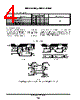
️· Propagation Delay (tPLH & tPHL): A critical parameter for digital circuits. Specifies the time delay between input and output signals.
- Values range from ~18ns to 32ns depending on the version (74LS398 vs 74LS398D).
️· Clock Pulse Width (tW): The clock signal needs to be high for at least 12ns to allow correct operation.
️· Data Setup Time (ts): The data must be stable for a certain period *before* the clock edge to be registered correctly. This value is 25ns.
️· Data Hold Time (th): The data must remain stable after the clock edge. A minimum of 0ns is stated.
️· These specifications give good indication of the speed the device operates at.
4. Package Information:
️· Multiple Package Types supported, including:
- SO-16 (D Suffix): Small Outline Integrated Circuit
- Ceramic DIP (J Suffix): Dual In-Line Package
- Plastic DIP (N Suffix): Standard Dual In-Line Package
️· Pinout diagrams are provided in the datasheet. The datasheet has the pin assignments described.
5. Important Notes/Disclaimers:
️· Motorola's Rights: Motorola reserves the right to make changes to the device specifications without notice.
️· Liability Disclaimer: Motorola disclaims any liability for improper use of the device, especially in life-critical applications.
️· Application Considerations: It emphasizes that typical parameters should be validated for each application.
️· Motorola Branding: The text acknowledges Motorola and emphasizes their policy towards equality.
️· Distribution Centers: The text provides details of distribution centers across different areas of the world.
In short, this datasheet details a standard 8-bit serial-in, parallel-out register for digital systems. It includes electrical characteristics, timing specifications, and packaging options. Always refer to the full datasheet for complete details and application guidance.
1. Device Overview:
️· Part Number: 74LS398 (multiple suffixes exist like 'D', 'J', 'N' influencing package type)
️· Type: 8-bit Data Register with 3-State Outputs
️· Function: This is a shift register. Data is shifted in serially and appears in parallel at the outputs. The 3-state outputs allow the register to be easily connected in series to create long shift register chains. It essentially takes a serial bit stream and converts it into a parallel byte.
️· Key Features:
- Serial data input
- Parallel data output
- 3-state outputs (active high, enabled by a control signal)
- Allows cascading for extended data shifting
- Standard LS TTL compatibility
2. Key Specifications (DC Characteristics):
️· Supply Voltage (VCC):
- 74LS398: 5.0V to 5.5V
- 74LS398D: 4.5V to 5.5V
️· Input HIGH Voltage (VIH):
- 74LS398: 2.0V
- 74LS398D: 2.0V
️· Input LOW Voltage (VIL):
- 74LS398: 0.8V
- 74LS398D: 0.8V
️· Output HIGH Voltage (VOH):
- VCC = 5.0V, IOH = -4.0mA (74LS398) / -8.0mA (74LS398D)
️· Output LOW Voltage (VOL):
- IOL = 8.0mA (74LS398D) / 4.0mA (74LS398)
️· Input Current (IIH & IIL): Specifies the current drawn into the inputs.
️· Power Supply Current (ICC): A typical value of 13mA is given.
3. Timing Characteristics (AC):
️· Propagation Delay (tPLH & tPHL): A critical parameter for digital circuits. Specifies the time delay between input and output signals.
- Values range from ~18ns to 32ns depending on the version (74LS398 vs 74LS398D).
️· Clock Pulse Width (tW): The clock signal needs to be high for at least 12ns to allow correct operation.
️· Data Setup Time (ts): The data must be stable for a certain period *before* the clock edge to be registered correctly. This value is 25ns.
️· Data Hold Time (th): The data must remain stable after the clock edge. A minimum of 0ns is stated.
️· These specifications give good indication of the speed the device operates at.
4. Package Information:
️· Multiple Package Types supported, including:
- SO-16 (D Suffix): Small Outline Integrated Circuit
- Ceramic DIP (J Suffix): Dual In-Line Package
- Plastic DIP (N Suffix): Standard Dual In-Line Package
️· Pinout diagrams are provided in the datasheet. The datasheet has the pin assignments described.
5. Important Notes/Disclaimers:
️· Motorola's Rights: Motorola reserves the right to make changes to the device specifications without notice.
️· Liability Disclaimer: Motorola disclaims any liability for improper use of the device, especially in life-critical applications.
️· Application Considerations: It emphasizes that typical parameters should be validated for each application.
️· Motorola Branding: The text acknowledges Motorola and emphasizes their policy towards equality.
️· Distribution Centers: The text provides details of distribution centers across different areas of the world.
In short, this datasheet details a standard 8-bit serial-in, parallel-out register for digital systems. It includes electrical characteristics, timing specifications, and packaging options. Always refer to the full datasheet for complete details and application guidance.
| Part No. | SN54LS398 |
| Manufacturer | MOTOROLA |
| Size | 209 Kbytes |
| Pages | 6 pages |
| Description | QUAD 2-PORT REGISTER |
| War ALLDATASHEET hilfreich? [ DONATE ] |
Über Alldatasheet | Werbung | Kontakt | Privatsphäre und Datenschutz | Link zum Datenblatt | Linktausch | Hersteller All Rights Reserved©Alldatasheet.com |
| Russian : Alldatasheetru.com | Korean : Alldatasheet.co.kr | Spanish : Alldatasheet.es | French : Alldatasheet.fr | Italian : Alldatasheetit.com Portuguese : Alldatasheetpt.com | Polish : Alldatasheet.pl | Vietnamese : Alldatasheet.vn Indian : Alldatasheet.in | Mexican : Alldatasheet.com.mx | British : Alldatasheet.co.uk | New Zealand : Alldatasheet.co.nz |
|
Family Site : ic2ic.com |
icmetro.com |
 German ▼
  English
 Chinese
 Japanese
 Russian
 Korean
 Spanish
 French
 Italian
 Portuguese
 Polish
 Vietnamese
 Indian
 Mexican
 British
 New Zealand