|
Datenblatt-Suchmaschine für elektronische Bauteile |
|
|
Datenblatt-Suchmaschine für elektronische Bauteile |
|
SN54LS398 Datenblatt(PDF) 2 Page - Motorola, Inc |
|
|
|||||||||||||||||||||||||||||
SN54LS398 Datenblatt(HTML) 2 Page - Motorola, Inc |
|
|
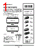
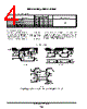
2 / 6 page  5-558 FAST AND LS TTL DATA SN54/74LS398 • SN54/74LS399 FUNCTIONAL BLOCK DIAGRAM IOA S IIA IOB IIB IOC IIC IOD IID S S S S R R R R QA QA QB QB QC QC QD QD * * * * * SN54 / 74LS398 only FUNCTIONAL DESCRIPTION The SN54 / 74LS398 and SN54 / 74LS399 are high-speed Quad 2-Port Registers. They select four bits of data from two sources (Ports) under the control of a common Select Input (S). The selected data is transferred to a 4-Bit Output Register synchronous with the LOW-to-HIGH transition of the Clock in- put (CP). The 4-Bit RS type output register is fully edge-trig- gered. The Data inputs (I) and Select inputs (S) must be stable only a setup time prior to and hold time after the LOW-to-HIGH transition of the Clock input for predictable operation. The SN54 / 74LS398 has both Q and Q Outputs available. FUNCTION TABLE INPUTS OUTPUTS S I0 I1 Q Q* I I X L H I h X H L h X I L H h X h H L *SN54 / 74LS398 only I = LOW Voltage Level one setup time pior to the LOW-to-HIGH clock transition h = HIGH Voltage Level one setup time prior to the LOW-to-HIGH clock transition L = LOW Voltage Level H = HIGH Voltage Level X = Immaterial |
|
|
Link URL |
| War ALLDATASHEET hilfreich? [ DONATE ] |
Über Alldatasheet | Werbung | Kontakt | Privatsphäre und Datenschutz | Link zum Datenblatt | Linktausch | Hersteller All Rights Reserved©Alldatasheet.com |
| Russian : Alldatasheetru.com | Korean : Alldatasheet.co.kr | Spanish : Alldatasheet.es | French : Alldatasheet.fr | Italian : Alldatasheetit.com Portuguese : Alldatasheetpt.com | Polish : Alldatasheet.pl | Vietnamese : Alldatasheet.vn Indian : Alldatasheet.in | Mexican : Alldatasheet.com.mx | British : Alldatasheet.co.uk | New Zealand : Alldatasheet.co.nz |
|
Family Site : ic2ic.com |
icmetro.com |
 German ▼
 English
 Chinese
 German
 Japanese
 Russian
 Korean
 Spanish
 French
 Italian
 Portuguese
 Polish
 Vietnamese
 Indian
 Mexican
 British
 New Zealand