 |
Datenblatt-Suchmaschine für elektronische Bauteile |
|
|
Datenblatt-Suchmaschine für elektronische Bauteile |
|
The question interval is too short.
Please try again in a few seconds.

Hello, Please ask a question about 54AC02L Datasheet
# Example questions:
➢ What is the maximum storage temperature specified for the 54ac series?
➢ What is the minimum high-level input voltage (vih) at a vcc of 4.5v?
➢ What is the maximum dynamic output current (iohd) specified for the 54ac series?
| Part No. | 54AC02L |
| Manufacturer | NSC |
| Size | 111 Kbytes |
| Pages | 6 pages |
| Description | Quad 2-Input NOR Gate |



1. General Description & Purpose
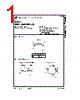
️· This document describes the National Semiconductor 54AC series logic gates. These are standard logic gates, offering a balance of speed and power consumption.
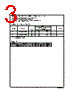
️· The datasheet provides electrical characteristics, AC performance data, and recommended operating conditions for the gates.
️· It explicitly *does not* cover all possible package options (it refers to Ceramic DIP, Flatpack, and Leadless Chip Carrier, but doesn't show all variations).
️· Crucially: The specific logic function (NAND, NOR, etc.) is *not* explicitly stated within the datasheet itself. This suggests it's a generalized datasheet covering several 54AC gate types.
2. Absolute Maximum Ratings (Operating Conditions)
️· Supply Voltage (Vcc): -0.5V to +7.0V (Important: Exceeding the maximum voltage can permanently damage the device.)
️· Input/Output Voltages (Vi/Vo): -0.5V to Vcc + 0.5V (Must stay within this range to avoid damage.)
️· Input Diode Current (Iik): -20mA to +20mA (Max current through input diodes.)
️· Output Diode Current (Iok): -20mA to +20mA (Max current through output diodes.)
️· Storage Temperature: -65°C to +150°C (Range for storage, not operating)
️· Junction Temperature (Tj): 175°C (Important for thermal management)
3. Recommended Operating Conditions
️· Supply Voltage (Vcc): 2.0V to 6.0V (This is the "sweet spot" for reliable operation)
️· Input Voltage (Vi): 0V to Vcc
️· Output Voltage (Vo): 0V to Vcc
️· Operating Temperature (Ta): -55°C to +125°C
️· Input Edge Rate (dV/dt): Minimum 125 mV/ns. (This specifies how quickly input signals can change)
4. Electrical Characteristics (DC)
️· Input Voltages (Vih, Vil): These define the voltage levels required for a logic input to be recognized as a '1' or a '0', respectively. Values vary depending on Vcc.
️· Output Voltages (Voh, Vol): These define the voltage levels at the output when the input(s) represent a logic '1' or a logic '0'.
️· Input Leakage Current (Iin): A small current that can flow into the input when it's not actively driven.
️· Quiescent Supply Current (Icc): The supply current when the gate is not switching.
5. AC Electrical Characteristics
️· Propagation Delay Time (tPLH, tPHL): These are the critical parameters defining how long it takes for a change in input to propagate to the output. Values depend on Vcc.
️· Rise and Fall Times: These describe how quickly the output signal transitions between logic levels.
6. Package Information
️· The datasheet references several package types:
- Ceramic Dual In-line Package (DIP)
- Ceramic Flatpack
- Leadless Chip Carrier (LCC)
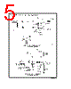
️· The dimensional information for specific packages is shown in separate diagrams within the document.
7. Important Notes
️· Life Support Policy: National Semiconductor devices are not approved for use in life-support systems without prior written approval.
️· Disclaimer: National Semiconductor is not responsible for the use of its devices in any circuits or systems.
1. General Description & Purpose
️· This document describes the National Semiconductor 54AC series logic gates. These are standard logic gates, offering a balance of speed and power consumption.
️· The datasheet provides electrical characteristics, AC performance data, and recommended operating conditions for the gates.
️· It explicitly *does not* cover all possible package options (it refers to Ceramic DIP, Flatpack, and Leadless Chip Carrier, but doesn't show all variations).
️· Crucially: The specific logic function (NAND, NOR, etc.) is *not* explicitly stated within the datasheet itself. This suggests it's a generalized datasheet covering several 54AC gate types.
2. Absolute Maximum Ratings (Operating Conditions)
️· Supply Voltage (Vcc): -0.5V to +7.0V (Important: Exceeding the maximum voltage can permanently damage the device.)
️· Input/Output Voltages (Vi/Vo): -0.5V to Vcc + 0.5V (Must stay within this range to avoid damage.)
️· Input Diode Current (Iik): -20mA to +20mA (Max current through input diodes.)
️· Output Diode Current (Iok): -20mA to +20mA (Max current through output diodes.)
️· Storage Temperature: -65°C to +150°C (Range for storage, not operating)
️· Junction Temperature (Tj): 175°C (Important for thermal management)
3. Recommended Operating Conditions
️· Supply Voltage (Vcc): 2.0V to 6.0V (This is the "sweet spot" for reliable operation)
️· Input Voltage (Vi): 0V to Vcc
️· Output Voltage (Vo): 0V to Vcc
️· Operating Temperature (Ta): -55°C to +125°C
️· Input Edge Rate (dV/dt): Minimum 125 mV/ns. (This specifies how quickly input signals can change)
4. Electrical Characteristics (DC)
️· Input Voltages (Vih, Vil): These define the voltage levels required for a logic input to be recognized as a '1' or a '0', respectively. Values vary depending on Vcc.
️· Output Voltages (Voh, Vol): These define the voltage levels at the output when the input(s) represent a logic '1' or a logic '0'.
️· Input Leakage Current (Iin): A small current that can flow into the input when it's not actively driven.
️· Quiescent Supply Current (Icc): The supply current when the gate is not switching.
5. AC Electrical Characteristics
️· Propagation Delay Time (tPLH, tPHL): These are the critical parameters defining how long it takes for a change in input to propagate to the output. Values depend on Vcc.
️· Rise and Fall Times: These describe how quickly the output signal transitions between logic levels.
6. Package Information
️· The datasheet references several package types:
- Ceramic Dual In-line Package (DIP)
- Ceramic Flatpack
- Leadless Chip Carrier (LCC)
️· The dimensional information for specific packages is shown in separate diagrams within the document.
7. Important Notes
️· Life Support Policy: National Semiconductor devices are not approved for use in life-support systems without prior written approval.
️· Disclaimer: National Semiconductor is not responsible for the use of its devices in any circuits or systems.
| Part No. | 54AC02L |
| Manufacturer | NSC |
| Size | 111 Kbytes |
| Pages | 6 pages |
| Description | Quad 2-Input NOR Gate |
| War ALLDATASHEET hilfreich? [ DONATE ] |
Über Alldatasheet | Werbung | Kontakt | Privatsphäre und Datenschutz | Link zum Datenblatt | Linktausch | Hersteller All Rights Reserved©Alldatasheet.com |
| Russian : Alldatasheetru.com | Korean : Alldatasheet.co.kr | Spanish : Alldatasheet.es | French : Alldatasheet.fr | Italian : Alldatasheetit.com Portuguese : Alldatasheetpt.com | Polish : Alldatasheet.pl | Vietnamese : Alldatasheet.vn Indian : Alldatasheet.in | Mexican : Alldatasheet.com.mx | British : Alldatasheet.co.uk | New Zealand : Alldatasheet.co.nz |
|
Family Site : ic2ic.com |
icmetro.com |
 German ▼
  English
 Chinese
 Japanese
 Russian
 Korean
 Spanish
 French
 Italian
 Portuguese
 Polish
 Vietnamese
 Indian
 Mexican
 British
 New Zealand