|
Datenblatt-Suchmaschine für elektronische Bauteile |
|
|
Datenblatt-Suchmaschine für elektronische Bauteile |
|
MP2374 Datenblatt(PDF) 8 Page - Monolithic Power Systems |
|
|
|||||||||||||||||||||||||||||
MP2374 Datenblatt(HTML) 8 Page - Monolithic Power Systems |
|
|
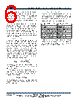
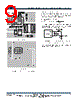
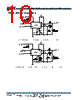
8 / 11 page  MP2374 – 6.5V-32V INPUT, 1A, 330kHz STEP-DOWN CONVERTER MP2374 Rev. 1.0 www.MonolithicPower.com 8 1/23/2014 MPS Proprietary Information. Patent Protected. Unauthorized Photocopy and Duplication Prohibited. © 2014 MPS. All Rights Reserved. To optimize the compensation components that are not listed in Table 4, use the following procedure. Choose the compensation resistor to set the desired crossover frequency. Determine the value by the following equation: REF CS EA C OUT V G G f V 5 C 2 3 R × × × × × π = Putting in the know constants and setting the crossover frequency to the desired 33KHz: OUT 7 V 5 C 10 88 . 6 3 R × × × ≅ Choose the compensation capacitor to set the zero below one fourth of the crossover frequency. Determine the value by the following equation: 3 R 10 93 . 1 f 3 R 2 4 C 5 C − × ≈ × × π > Determine if the second compensation capacitor, C3, is required. It is required if the ESR zero of the output capacitor occurs at less than four times the crossover frequency, or 1 f R 5 C 8 C ESR ≥ × × × π If this is the case, then add the second compensation resistor. Determine the value by the equation: 3 R R 5 C 3 C ) MAX ( ESR × = Where RESR(MAX) is the maximum ESR of the output capacitor. Example: VOUT = 5V, C5 = 22μF Ceramic (ESR = 10mΩ) R3 ≈ 6.88x10⁷ (22x10-6) (5) = 7568Ω Use the nearest standard value of 7.5kΩ. C4 > 1.93x10⁻⁵ / 7.5K = 2.57nF Use standard value of 2.7nF. 8π x C5 x RESR x fC = 0.22, which is less than 1. Therefore, no second compensation capacitor (C3) is required. PCB Layout Guide PCB layout is very important to achieve stable operation. Please follow these guidelines and take Figure2 and 3 for references. 1) Keep the path of switching current short and minimize the loop area formed by Input cap, high-side and low-side MOSFETs. 2) Keep the connection of low-side MOSFET between SW pin and input power ground as short and wide as possible. 3) Ensure all feedback connections are short and direct. Place the feedback resistors and compensation components as close to the chip as possible. 4) Route SW away from sensitive analog areas such as FB. 5) Connect IN, SW, and especially GND respectively to a large copper area to cool the chip to improve thermal performance and long-term reliability. For single layer, do not solder exposed pad of the IC Figure 2―PCB Layout (Single Layer) |
|
|
Link URL |
| War ALLDATASHEET hilfreich? [ DONATE ] |
Über Alldatasheet | Werbung | Kontakt | Privatsphäre und Datenschutz | Link zum Datenblatt | Linktausch | Hersteller All Rights Reserved©Alldatasheet.com |
| Russian : Alldatasheetru.com | Korean : Alldatasheet.co.kr | Spanish : Alldatasheet.es | French : Alldatasheet.fr | Italian : Alldatasheetit.com Portuguese : Alldatasheetpt.com | Polish : Alldatasheet.pl | Vietnamese : Alldatasheet.vn Indian : Alldatasheet.in | Mexican : Alldatasheet.com.mx | British : Alldatasheet.co.uk | New Zealand : Alldatasheet.co.nz |
|
Family Site : ic2ic.com |
icmetro.com |
 German ▼
 English
 Chinese
 German
 Japanese
 Russian
 Korean
 Spanish
 French
 Italian
 Portuguese
 Polish
 Vietnamese
 Indian
 Mexican
 British
 New Zealand