|
Datenblatt-Suchmaschine für elektronische Bauteile |
|
|
Datenblatt-Suchmaschine für elektronische Bauteile |
|
ADA4558WHCPZ-R7 Datenblatt(PDF) 11 Page - Analog Devices |
|
|
|||||||||||||||||||||||||||||
ADA4558WHCPZ-R7 Datenblatt(HTML) 11 Page - Analog Devices |
|
|
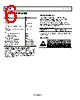
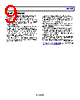
11 / 12 page  Data Sheet ADA4558 Rev. 0 | Page 11 of 12 PCB LAYOUT GUIDELINES Figure 5. Example PCB Layout The following items outline best practice for PCB layout. • Place the 220 pF CLIN capacitor close to the IC between the LIN and LINGND traces. • Place the CREG, CIN, and C1_8V capacitors close to the IC using short, thick tracks. These components decouple the supplies and reduce high frequency noise on these nodes. • The length of the C1_8V traces is critical. Keep the traces as short as possible. • Shield the noisy DVDD regulator pin from the sensitive analog circuitry at VPOS, VNEG, and VREG. • Maintain shielded matched differential lines for VNEG and VPOS to ensure that noise pickup is both minimal and common mode. The PGA can potentially obtain significant noise at this point. • Shield the VPOS trace from the VREG trace because VREG can have noise pickup during EMC testing. • Shield the VDD12 line from VPOS, VNEG, and VREG using a ground plane. • Connect DGND and LINGND to AGND at a single point. Use a short narrow trace for DGND and a wide trace for LINGND. • TESTD is connected internally to DGND. Connect Pin 3 to a small DGND plane to avoid multiple connections between AGND and DGND. • To minimize total ground plane impedance, use a separate ground layer, if available, with many via connections to the top layer ground plane. • When a second routing layer is available, the LINGND trace can be connected to the AGND plane with a large via close to CDVDD. Connect DGND to AGND at this point with a narrow trace. |
|
|
Link URL |
| War ALLDATASHEET hilfreich? [ DONATE ] |
Über Alldatasheet | Werbung | Kontakt | Privatsphäre und Datenschutz | Link zum Datenblatt | Linktausch | Hersteller All Rights Reserved©Alldatasheet.com |
| Russian : Alldatasheetru.com | Korean : Alldatasheet.co.kr | Spanish : Alldatasheet.es | French : Alldatasheet.fr | Italian : Alldatasheetit.com Portuguese : Alldatasheetpt.com | Polish : Alldatasheet.pl | Vietnamese : Alldatasheet.vn Indian : Alldatasheet.in | Mexican : Alldatasheet.com.mx | British : Alldatasheet.co.uk | New Zealand : Alldatasheet.co.nz |
|
Family Site : ic2ic.com |
icmetro.com |
 German ▼
 English
 Chinese
 German
 Japanese
 Russian
 Korean
 Spanish
 French
 Italian
 Portuguese
 Polish
 Vietnamese
 Indian
 Mexican
 British
 New Zealand