|
Datenblatt-Suchmaschine für elektronische Bauteile |
|
|
Datenblatt-Suchmaschine für elektronische Bauteile |
|
PA94 Datenblatt(PDF) 4 Page - Cirrus Logic |
|
|
|||||||||||||||||||||||||||||
PA94 Datenblatt(HTML) 4 Page - Cirrus Logic |
|
|
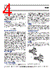
4 / 4 page  APEX MICROTECHNOLOGY CORPORATION • 5980 NORTH SHANNON ROAD • TUCSON, ARIZONA 85741 • USA • APPLICATIONS HOTLINE: 1 (800) 546-2739 4 GENERAL Please read Application Note 1 "General Operating Con- siderations" which covers stability, supplies, heat sinking, mounting, current limit, SOA interpretation, and specification interpretation. Visit www.apexmicrotech.com for design tools that help automate tasks such as calculations for stability, internal power dissipation, current limit; heat sink selection; Apex’s complete Application Notes library; Technical Seminar Workbook; and Evaluation Kits. CURRENT LIMIT For proper operation, the current limit resistor (R LIM) must be connected as shown in the external connection diagram. The minimum value is 3.5 ohm, however for optimum reliability the resistor value should be set as high as possible. The value is calculated as follows; with the maximum practical value of 30 ohms. .7 R LIM = I LIM COMMON MODE INPUT RANGE Operational amplifiers are usually designed to have a com- mon mode input voltage range that approximates the power supply voltage range. However, to keep the cost as low as possible and still meet the requirements of most applications the common mode input voltage range of the PA94 is restricted. The input pins must always be a least 30V from either supply voltage but never more than 450V. This means that the PA94 cannot be used in applications where the supply voltages are extremely unbalanced. For example, supply voltages of +800V and –100V would not be allowed in an application where the non-inverting pin is grounded because in normal operation both input pins would be at 0V and the difference voltage between the positive supply and the input pins would be 800V. In this kind of application, however, supply voltages +450V and -100V does meet the input common mode voltage range requirements since the maximum difference voltage between the inputs pins and the supply voltage is 450V (the maximum allowed). The output has no such restrictions on its voltage swing. The output can swing within 24V of either supply voltage regardless of value so long as the total supply voltage does not exceed 900V. INPUT PROTECTION Although the PA94 can withstand differential input voltages up to ±20V, additional external protection is recommended. In most applications 1N4148 or 1N914 signal diodes are sufficient (D1, D2 in Figure 1a). In more demanding applications where low leakage or low capacitance are of concern 2N4416 or 2N5457-2N5459 JFETs connected as diodes will be required (Q1, Q2 in Figure 1b). In either case the input differential voltage will be clamped to ±.7V. This is sufficient overdrive to produce maximum power bandwidth. Note that this protection does not automatically protect the amplifier from excessive common mode input voltages. POWER SUPPLY PROTECTION Unidirectional zener diode transient suppressors are recom- mended as protection on the supply pins. The zeners clamp transients to voltages within the power supply rating and also clamp power supply reversals to ground. Whether the zeners are used or not, the system power supply should be evaluated for transient performance including power-on overshoot and power-off polarity reversal as well as line regulation. Conditions which can cause open circuits or polarity reversals on either power supply rail should be avoided or protected against. Reversals or opens on the negative supply rail is known to induce input stage failure. Unidirectional transzorbs prevent this, and it is desirable that they be both electrically and physically as close to the amplifier as possible. STABILITY The PA94 is stable at gains of 100 or more with a NPO (COG) compensation capacitor of 2.2pF. The compensation capaci- tor, Cc, in the external connections diagram must be rated at 1000V working voltage and mounted closely to pins 4 and 6 to prevent spurious oscillation. A compensation capacitor less than 2.2pF is not recommended. EXTERNAL COMPONENTS The compensation capacitor Cc must be rated for the total supply voltage. An NPO (COG) capacitor rated a 1kV is rec- ommended. Of equal importance are the voltage rating and voltage co- efficient of the gain setting feedback resistor. Typical voltage ratings of low wattage resistors are 150 to 250V. Up to 500 V can appear across the feedback resistor. High voltage rated resistors can be obtained. However a 1 megohm feedback resistor composed of five 200k resistors in series will produce the proper voltage rating. CAUTIONS The operating voltages of the PA94 are potentially lethal. During circuit design develop a functioning circuit at the lowest possible voltages. Clip test leads should be used for "hands off" measurements while troubleshooting. FIGURE 1. OVERVOLTAGE PROTECTION ���� ��� ��� ��� �� �� �� �� �� �� � � ��� ��� ��� �� �� �� �� � � ���� �� �� �� �� ��� ��� PA94 OPERATING CONSIDERATIONS This data sheet has been carefully checked and is believed to be reliable, however, no responsibility is assumed for possible inaccuracies or omissions. All specifications are subject to change without notice. PA94U REV J APRIL 2005 © 2005 Apex Microtechnology Corp. |
|
|
Link URL |
| War ALLDATASHEET hilfreich? [ DONATE ] |
Über Alldatasheet | Werbung | Kontakt | Privatsphäre und Datenschutz | Link zum Datenblatt | Linktausch | Hersteller All Rights Reserved©Alldatasheet.com |
| Russian : Alldatasheetru.com | Korean : Alldatasheet.co.kr | Spanish : Alldatasheet.es | French : Alldatasheet.fr | Italian : Alldatasheetit.com Portuguese : Alldatasheetpt.com | Polish : Alldatasheet.pl | Vietnamese : Alldatasheet.vn Indian : Alldatasheet.in | Mexican : Alldatasheet.com.mx | British : Alldatasheet.co.uk | New Zealand : Alldatasheet.co.nz |
|
Family Site : ic2ic.com |
icmetro.com |
 German ▼
 English
 Chinese
 German
 Japanese
 Russian
 Korean
 Spanish
 French
 Italian
 Portuguese
 Polish
 Vietnamese
 Indian
 Mexican
 British
 New Zealand