|
Datenblatt-Suchmaschine für elektronische Bauteile |
|
|
Datenblatt-Suchmaschine für elektronische Bauteile |
|
LP3942YQ Datenblatt(PDF) 7 Page - National Semiconductor (TI) |
|
|
|
|||||||||||||||||||||||||||||
LP3942YQ Datenblatt(HTML) 7 Page - National Semiconductor (TI) |
|
|
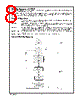
7 / 20 page  SPI Interface LP3942 is compatible with SPI serial bus specification and it operates as a write-only slave. One write cycle consists of 7 Address bits, 1 Read/Write (RW, always high) bit and 8 Data bits. The Address and Data are transmitted MSB first. The Slave Select signal SS must be low during the Cycle transmission. SS resets the interface when high and it has to be taken high between successive Cycles. Data is clocked in on the rising edge of the SCK clock signal. 20129205 SPI Write Cycle 20129206 SPI Timing Diagram SPI TIMING PARAMETERS Symbol Parameter Limit Units Min Max 1 Cycle Time 80 - ns 2 Enable Lead Time 5 - ns 3 Enable Lag Time 5 - ns 4 Clock Low Time 35 - ns 5 Clock High Time 35 - ns 6 Data Setup Time 15 - ns 7 Data Hold Time 10 - ns 8 SS Inactive Time 40 - ns Charge Pump Mode Selection Charge pump mode is controlled through the SPI interface. The mode selection is shown in the following tables. Addr. Reg. [7] [6] [5] [4] [3] [2] [1] [0] 02’h CTRL NSTBY CP_ON CC/SW2 CC/SW1 1.5x/2x reserved reserved reserved default 0 0 0 0 0 0 0 0 Control Bit Parameter State Function NSTBY Low Active Standby NSTBY = 0 LP3942 is disabled NSTBY = 1 LP3942 is active CP_ON Charge Pump Enable CP_ON = 0 Charge Pump is disabled CP_ON = 1 Charge Pump is active 1.5x/2x Charge Pump Mode 1.5x/2x 1.5x/2x = 0 1.5x mode, V OUT = 4.5V 1.5x/2x = 1 2x mode, V OUT =5V If charge pump is disabled (CP_ON = 0) and LP3942 is active (NSTBY = 1), then charge pump output (P OUT) pin must be connected externally to the same supply voltage (max 5.0V) which is used to drive LEDs with RGB1 or RGB2 outputs. www.national.com 7 |
|
|
Link URL |
| War ALLDATASHEET hilfreich? [ DONATE ] |
Über Alldatasheet | Werbung | Kontakt | Privatsphäre und Datenschutz | Link zum Datenblatt | Linktausch | Hersteller All Rights Reserved©Alldatasheet.com |
| Russian : Alldatasheetru.com | Korean : Alldatasheet.co.kr | Spanish : Alldatasheet.es | French : Alldatasheet.fr | Italian : Alldatasheetit.com Portuguese : Alldatasheetpt.com | Polish : Alldatasheet.pl | Vietnamese : Alldatasheet.vn Indian : Alldatasheet.in | Mexican : Alldatasheet.com.mx | British : Alldatasheet.co.uk | New Zealand : Alldatasheet.co.nz |
|
Family Site : ic2ic.com |
icmetro.com |
 German ▼
 English
 Chinese
 German
 Japanese
 Russian
 Korean
 Spanish
 French
 Italian
 Portuguese
 Polish
 Vietnamese
 Indian
 Mexican
 British
 New Zealand