|
Datenblatt-Suchmaschine für elektronische Bauteile |
|
|
Datenblatt-Suchmaschine für elektronische Bauteile |
|
400EABAA2 Datenblatt(PDF) 5 Page - ON Semiconductor |
|
|
|||||||||||||||||||||||||||||
400EABAA2 Datenblatt(HTML) 5 Page - ON Semiconductor |
|
|
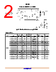
5 / 47 page  NCP12400 www.onsemi.com 5 Table 4. MAXIMUM RATINGS Rating Symbol Value Unit DRV (pin 5) Maximum voltage on DRV pin (Dc−Current self−limited if operated within the allowed range) (Note 2) –0.3 to 20 ±1000 (peak) V mA VCC (pin 6) VCCPower Supply voltage, VCC pin, continuous voltage Power Supply voltage, VCC pin, continuous voltage (Note 2) –0.3 to 36 ±30 (peak) V mA HV (pin 8) Maximum voltage on HV pin (Dc−Current self−limited if operated within the allowed range) –0.3 to 750 ±20 V mA Vmax Maximum voltage on low power pins (except pin 5, pin 6 and pin 8) (Dc−Current self−limited if operated within the allowed range) (Note 2) –0.3 to 5.5 ±10 (peak) V mA RqJ−A Thermal Resistance SOIC−7 Junction-to-Air, low conductivity PCB (Note 3) Junction-to-Air, medium conductivity PCB (Note 4) Junction-to-Air, high conductivity PCB (Note 5) 162 147 115 °C/W RqJ−C Thermal Resistance Junction−to−Case 73 °C/W TJMAX Operating Junction Temperature −40 to +150 °C TSTRGMAX Storage Temperature Range −60 to +150 °C ESD Capability, HBM model (All pins except HV) (Note 1) > 4000 V ESD Capability, HBM model (pin 8, HV) > 2000 V ESD Capability, Charge Discharge Model (Note 1) > 500 V Stresses exceeding those listed in the Maximum Ratings table may damage the device. If any of these limits are exceeded, device functionality should not be assumed, damage may occur and reliability may be affected. 1. This device series contains ESD protection and exceeds the following tests: Human Body Model 4000 V per JEDEC standard JESD22, Method A114E Charge Discharge Model Method 500 V per JEDEC standard JESD22, Method C101E 2. This device contains latch-up protection and exceeds 100 mA per JEDEC Standard JESD78. 3. As mounted on a 80 x 100 x 1.5 mm FR4 substrate with a single layer of 50 mm2 of 2 oz copper traces and heat spreading area. As specified for a JEDEC 51-1 conductivity test PCB. Test conditions were under natural convection or zero air flow. 4. As mounted on a 80 x 100 x 1.5 mm FR4 substrate with a single layer of 100 mm2 of 2 oz copper traces and heat spreading area. As specified for a JEDEC 51-2 conductivity test PCB. Test conditions were under natural convection or zero air flow. 5. As mounted on a 80 x 100 x 1.5 mm FR4 substrate with a single layer of 650 mm2 of 2 oz copper traces and heat spreading area. As specified for a JEDEC 51-3 conductivity test PCB. Test conditions were under natural convection or zero air flow. Table 5. ELECTRICAL CHARACTERISTICS (For typical values TJ = 25°C, for min/max values TJ = −40°C to +125°C, VHV = 125 V, VCC = 11 V unless otherwise noted) Characteristics Test Condition Symbol Min Typ Max Unit HIGH VOLTAGE CURRENT SOURCE Minimum voltage for current source operation VHV(min) − 30 40 V Current flowing out of VCC pin VCC = 0 V VCC = VCC(on) − 0.5 V Istart1 Istart2 0.2 5 0.5 8 0.8 11 mA Off−state leakage current VHV = 750 V, VCC = 15 V Istart(off) − 2 6 mA SUPPLY Turn−on threshold level, VCC going up HV current source stop threshold (depending on the version) VCC(on) 11.0 15.0 12.0 16.2 13.0 17.5 V HV current source restart threshold VCC(min) 9.5 10.5 11.5 V Turn−off threshold VCC(off) 8.4 8.9 9.3 V Overvoltage threshold Overvoltage threshold (option EAHBB, BBBBB) VCC(ovp) 25 30 26.5 32 28 34 V Blanking duration on VCC(off) and VCC(ovp) detection tVCC(blank) − 10 − ms 6. Guaranteed by design. 7. CS pin source current is a sum of Ibias and IOPC, thus at VHV = 125 V is observed the Ibias only, because IOPC is switched off. |
|
Link URL |
| War ALLDATASHEET hilfreich? [ DONATE ] |
Über Alldatasheet | Werbung | Kontakt | Privatsphäre und Datenschutz | Link zum Datenblatt | Linktausch | Hersteller All Rights Reserved©Alldatasheet.com |
| Russian : Alldatasheetru.com | Korean : Alldatasheet.co.kr | Spanish : Alldatasheet.es | French : Alldatasheet.fr | Italian : Alldatasheetit.com Portuguese : Alldatasheetpt.com | Polish : Alldatasheet.pl | Vietnamese : Alldatasheet.vn Indian : Alldatasheet.in | Mexican : Alldatasheet.com.mx | British : Alldatasheet.co.uk | New Zealand : Alldatasheet.co.nz |
|
Family Site : ic2ic.com |
icmetro.com |
 German ▼
 English
 Chinese
 German
 Japanese
 Russian
 Korean
 Spanish
 French
 Italian
 Portuguese
 Polish
 Vietnamese
 Indian
 Mexican
 British
 New Zealand