|
Datenblatt-Suchmaschine für elektronische Bauteile |
|
|
Datenblatt-Suchmaschine für elektronische Bauteile |
|
CP152S Datenblatt(PDF) 6 Page - STMicroelectronics |
|
|
|||||||||||||||||||||||||||||
CP152S Datenblatt(HTML) 6 Page - STMicroelectronics |
|
|
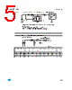
6 / 11 page  Technical information LCP1521S/LCP152DEE 6/11 2 Technical information Figure 5. LCP152 concept behavior Figure 5. shows the classical protection circuit using the LCP152 crowbar concept. This topology has been developed to protect the new high voltage SLICs. It allows to program the negative firing threshold while the positive clamping value is fixed at GND. When a negative surge occurs on one wire (L1 for example) a current IG flows through the base of the transistor T1 and then injects a current in the gate of the thyristor Th1. Th1 fires and all the surge current flows through the ground. After the surge when the current flowing through Th1 becomes less negative than the holding current IH, then Th1 switches off. When a positive surge occurs on one wire (L1 for example) the diode D1 conducts and the surge current flows through the ground. Figure 6. Example of PCB layout based on LCP152S protection Figure 6. shows the classical PCB layout used to optimize line protection. The capacitor C is used to speed up the crowbar structure firing during the fast surge edges. This allows to minimize the dynamical breakover voltage at the SLIC Tip and Ring inputs during fast strikes. Note that this capacitor is generally present around the SLIC - Vbat pin. So to be efficient it has to be as close as possible from the LCP152 Gate pin and from the reference ground track (or plan) (see Figure 6.). The optimized value for C is 220 nF. The series resitors Rs1 and Rs2 designed in Figure 5. represent the fuse resistors or the PTC which are mandatory to withstand the power contact or the power induction tests VRing GND Gate TIP RING GND -Vbat C Rs1 Rs2 L 1 L 2 V Tip Th1 D1 T1 IG ID1 To line side GND To SLIC side LCP1521S |
|
|
Link URL |
| War ALLDATASHEET hilfreich? [ DONATE ] |
Über Alldatasheet | Werbung | Kontakt | Privatsphäre und Datenschutz | Link zum Datenblatt | Linktausch | Hersteller All Rights Reserved©Alldatasheet.com |
| Russian : Alldatasheetru.com | Korean : Alldatasheet.co.kr | Spanish : Alldatasheet.es | French : Alldatasheet.fr | Italian : Alldatasheetit.com Portuguese : Alldatasheetpt.com | Polish : Alldatasheet.pl | Vietnamese : Alldatasheet.vn Indian : Alldatasheet.in | Mexican : Alldatasheet.com.mx | British : Alldatasheet.co.uk | New Zealand : Alldatasheet.co.nz |
|
Family Site : ic2ic.com |
icmetro.com |
 German ▼
 English
 Chinese
 German
 Japanese
 Russian
 Korean
 Spanish
 French
 Italian
 Portuguese
 Polish
 Vietnamese
 Indian
 Mexican
 British
 New Zealand