|
Datenblatt-Suchmaschine für elektronische Bauteile |
|
|
Datenblatt-Suchmaschine für elektronische Bauteile |
|
STDRIVE101TR Datenblatt(PDF) 19 Page - STMicroelectronics |
|
|
|||||||||||||||||||||||||||||
STDRIVE101TR Datenblatt(HTML) 19 Page - STMicroelectronics |
|
|
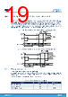
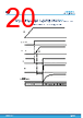
19 / 32 page  Important: If the 12 V regulator is bypassed, the consumption in standby mode is not reduced. The device enters standby mode keeping low all the driving input pins (INx/INHx and ENx/INLx) for at least tSTBY time. At power-up, if all the driving inputs are low, the device is immediately set in standby condition. The device leaves standby mode after a tWAKE time after at least one of the logic inputs is set high (refer to Figure 15 and Figure 16). Considering the standby condition disables the 12 V regulator, the device returns operative only after the REG12 voltage returns above the UVLO turn-on threshold. When the device exits from standby condition, the bootstrap capacitors charge via low-side turn-on is required, as described in Section 5.2.1.1 Figure 15. Standby and wake-up time (ENx/INx mode, with VS = VREG12 = 12 V) t 50% tSTBY off ENx INx GLSx GHSx 50% Device mode tWAKE Operative Operative Standby Standby 90% rising ONE of the 6 input lines the IC exits from standby GLS/GHS status according to ENx & INx inputs ton 10% Figure 16. Standby and wake-up time (INHx/INLx mode, with VS = VREG12 = 12 V) t 50% tSTBY off INxx GLSx GHSx 50% Device mode tWAKE Operative Operative Standby Standby 90% rising ONE of the 6 input lines the IC exits from standby GLS/GHS status according to INxx inputs ton 10% 5.5 Undervoltage protection The device provides UVLO protections on each power supply. During power-up (see Figure 17), the device leaves the UVLO condition when the respective supply voltage rises above the turn-on threshold. When the supply voltage is below the on-threshold voltage of a hysteresis, the UVLO condition is set. Table 9 summarizes which blocks are switched off in UVLO condition. Table 9. UVLO and OT protection management Block VREG12 UVLO VBOOTx UVLO HSU, HSV, HSW output LOW(1) LOW(1) (2) LSU, LSV, LSW output LOW(1) nFAULT open-drain output LOW OPEN STDRIVE101 Undervoltage protection DS13472 - Rev 1 page 19/32 |
|
Link URL |
| War ALLDATASHEET hilfreich? [ DONATE ] |
Über Alldatasheet | Werbung | Kontakt | Privatsphäre und Datenschutz | Link zum Datenblatt | Linktausch | Hersteller All Rights Reserved©Alldatasheet.com |
| Russian : Alldatasheetru.com | Korean : Alldatasheet.co.kr | Spanish : Alldatasheet.es | French : Alldatasheet.fr | Italian : Alldatasheetit.com Portuguese : Alldatasheetpt.com | Polish : Alldatasheet.pl | Vietnamese : Alldatasheet.vn Indian : Alldatasheet.in | Mexican : Alldatasheet.com.mx | British : Alldatasheet.co.uk | New Zealand : Alldatasheet.co.nz |
|
Family Site : ic2ic.com |
icmetro.com |
 German ▼
 English
 Chinese
 German
 Japanese
 Russian
 Korean
 Spanish
 French
 Italian
 Portuguese
 Polish
 Vietnamese
 Indian
 Mexican
 British
 New Zealand