|
Datenblatt-Suchmaschine für elektronische Bauteile |
|
|
Datenblatt-Suchmaschine für elektronische Bauteile |
|
V62C18164096 Datenblatt(PDF) 2 Page - Mosel Vitelic, Corp |
|
|
|||||||||||||||||||||||||||||
V62C18164096 Datenblatt(HTML) 2 Page - Mosel Vitelic, Corp |
|
|
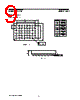
2 / 10 page  2 V62C18164096 Rev. 1.2 June 2000 MOSEL VITELIC V62C18164096 Pin Descriptions A0–A17 Address Inputs These 18 address inputs select one of the 256K x 16 bit segments in the RAM. CE1, CE2 Chip Enable Inputs CE1 is active LOW and CE2 is active HIGH. Both chip enables must be active to read from or write to the device. If either chip enable is not active, the device is deselected and is in a standby power mode. The I/O pins will be in the high-impedance state when deselected. OE Output Enable Input The output enable input is active LOW. With the chip enabled, when OE is Low and WE High, data will be presented on the I/O pins. The I/O pins will be in the high impedance state when OE is High. UBE, LBE Byte Enable Active low inputs. These inputs are used to enable the upper or lower data byte. WE Write Enable Input The write enable input is active LOW and controls read and write operations. With the chip enabled, when WE is HIGH and OE is LOW, output data will be present at the I/O pins; when WE is LOW and OE is HIGH, the data present on the I/O pins will be written into the selected memory locations. I/O1–I/O16 Data Input and Data Output Ports These 16 bidirectional ports are used to read data from and write data into the RAM. VCC Power Supply GND Ground Pin Configurations (Top View) 48 BGA A 1 234 56 1 Note: NC means no connect. 23 4 5 6 B C D E F G H TOP VIEW TOP VIEW A BLE I/O9 I/O10 B C D E F G H VSS VCC I/O15 I/O16 NC OE BHE I/O11 I/O12 I/O13 I/O14 NC A8 A0 A3 A5 A17 NC A14 A12 A9 A1 A4 A6 A7 A16 A15 A13 A10 A2 CE1 I/O2 I/O4 I/O5 I/O6 WE A11 CE2 I/O1 I/O3 VCC VSS I/O7 I/O8 NC |
|
|
Link URL |
| War ALLDATASHEET hilfreich? [ DONATE ] |
Über Alldatasheet | Werbung | Kontakt | Privatsphäre und Datenschutz | Link zum Datenblatt | Linktausch | Hersteller All Rights Reserved©Alldatasheet.com |
| Russian : Alldatasheetru.com | Korean : Alldatasheet.co.kr | Spanish : Alldatasheet.es | French : Alldatasheet.fr | Italian : Alldatasheetit.com Portuguese : Alldatasheetpt.com | Polish : Alldatasheet.pl | Vietnamese : Alldatasheet.vn Indian : Alldatasheet.in | Mexican : Alldatasheet.com.mx | British : Alldatasheet.co.uk | New Zealand : Alldatasheet.co.nz |
|
Family Site : ic2ic.com |
icmetro.com |
 German ▼
 English
 Chinese
 German
 Japanese
 Russian
 Korean
 Spanish
 French
 Italian
 Portuguese
 Polish
 Vietnamese
 Indian
 Mexican
 British
 New Zealand