|
Datenblatt-Suchmaschine für elektronische Bauteile |
|
|
Datenblatt-Suchmaschine für elektronische Bauteile |
|
ADP3415LRM-REEL7 Datenblatt(PDF) 2 Page - Analog Devices |
|
|
|||||||||||||||||||||||||||||
ADP3415LRM-REEL7 Datenblatt(HTML) 2 Page - Analog Devices |
|
|
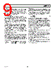
2 / 12 page  REV. B –2– ADP3415–SPECIFICATIONS1 (TA = 0 C to 100 C, VCC = 5 V, VBST – VSW = 5 V, SD = 5 V, CDRVH = CDRVL = 3 nF, unless otherwise noted.) Parameter Symbol Conditions Min Typ Max Unit SUPPLY (VCC) Quiescent Current 2 ICCQ Shutdown Mode VSD = 0.8 V 30 65 µA Operating Mode VSD = 5 V, No Switching 1.2 2 mA UNDERVOLTAGE LOCKOUT (UVLO) UVLO Threshold VCCUVLO 3.9 4.15 4.5 V UVLO Hysteresis VCCHUVLO 0.05 V LOW-SIDE DRIVER SHUTDOWN ( DRVLSD) Input Voltage High 3 VIH 2.0 V Input Voltage Low3 VIL 0.8 V Propagation Delay 3, 4 tpdlDRVLSD 20 50 ns (See Figure 3) tpdhDRVLSD 10 30 ns SHUTDOWN ( SD) Input Voltage High 3 VIH 2.0 V Input Voltage Low3 VIL 0.8 V INPUT (IN) Input Voltage High 3 VIH 2.0 V Input Voltage Low 3 VIL 0.8 V THERMAL SHUTDOWN (THSD) THSD Threshold TSD TJ = TA 165 °C THSD Hysteresis THSD TJ = TA 10 °C HIGH-SIDE DRIVER (DRVH) Output Resistance, DRVH–BST 1.5 3.5 Ω Output Resistance, DRVH–SW 0.85 2.0 Ω DRVH Transition Times 4 trDRVH VBST – VSW = 4.6 V 20 30 ns (See Figure 4) tfDRVH 25 35 ns DRVH Propagation Delay 4, 5 tpdhDRVH VBST – VSW = 4.6 V, VDLY = 0 V 10 22 40 ns RDLY ≥ 120 kΩ 100 200 ns (See Figure 4) tpdlDRVH 40 70 ns LOW-SIDE DRIVER (DRVL) Output Resistance, DRVL–VCC 1.6 3.0 Ω Output Resistance, DRVL–GND 1.0 3.0 Ω DRVL Transition Times 4 trDRVL VBST – VSW = 4.6 V 25 40 ns (See Figure 4) tfDRVL VBST – VSW = 4.6 V 20 30 ns DRVL Propagation Delay 4, 5, 6 tpdhDRVL VBST – VSW = 4.6 V 10 30 38 ns (See Figure 4) tpdlDRVL VBST – VSW = 4.6 V 10 25 ns SW Transition Timeout 7 tSWTO VBST – VSW = 4.6 V 130 300 ns Zero-Crossing Threshold VZC 1.6 V NOTES 1All limits at temperature extremes are guaranteed via correlation using standard Statistical Quality Control (SQC) methods. 2Including I BSTQ quiescent current. 3The signal source driving the pin must have 70 µA (typ) pull-down strength to make a high-to-low transient, and 20 µA (typ) pull-up strength to make a low-to-high transient. The pin does not represent load (<100 nA) in static low (<0.8 V) and static high (>2.0 V) logic states (see TPC 3.) The pin can be driven with standard TTL logic level source. 4Guaranteed by characterization. 5For propagation delays, tpdh refers to the specified signal going high, tpdl refers to it going low. 6Propagation delay measured until DRVL begins its transition. 7The turn-on of DRVL is initiated after IN goes low by either V SW crossing a ~1.6 V threshold or by expiration of t SWTO. Specifications subject to change without notice. |
|
|
Link URL |
| War ALLDATASHEET hilfreich? [ DONATE ] |
Über Alldatasheet | Werbung | Kontakt | Privatsphäre und Datenschutz | Link zum Datenblatt | Linktausch | Hersteller All Rights Reserved©Alldatasheet.com |
| Russian : Alldatasheetru.com | Korean : Alldatasheet.co.kr | Spanish : Alldatasheet.es | French : Alldatasheet.fr | Italian : Alldatasheetit.com Portuguese : Alldatasheetpt.com | Polish : Alldatasheet.pl | Vietnamese : Alldatasheet.vn Indian : Alldatasheet.in | Mexican : Alldatasheet.com.mx | British : Alldatasheet.co.uk | New Zealand : Alldatasheet.co.nz |
|
Family Site : ic2ic.com |
icmetro.com |
 German ▼
 English
 Chinese
 German
 Japanese
 Russian
 Korean
 Spanish
 French
 Italian
 Portuguese
 Polish
 Vietnamese
 Indian
 Mexican
 British
 New Zealand