|
Datenblatt-Suchmaschine für elektronische Bauteile |
|
|
Datenblatt-Suchmaschine für elektronische Bauteile |
|
N74F164D-T Datenblatt(PDF) 2 Page - NXP Semiconductors |
|
|
|||||||||||||||||||||||||||||
N74F164D-T Datenblatt(HTML) 2 Page - NXP Semiconductors |
|
|
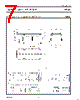
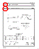
2 / 10 page  Philips Semiconductors Product specification 74F164 8-bit serial-in parallel-out shift register 2 2000 Dec 18 853-0348 25264 FEATURES • Gated serial data inputs • Typical shift frequency of 100MHz • Asynchronous Master Reset • Buffered clock and data inputs • Fully synchronous data transfer • Industrial temperature range available (–40 to +85 °C) DESCRIPTION The 74F164 is an 8-bit edge-triggered shift register with serial data entry and an output from each of the eight stages. Data is entered through one of two inputs (Dsa, Dsb); either input can be used as an active High enable for data entry through the other input. Both inputs must be connected together or an unused input must be tied High. Data shifts one place to the right on each Low-to-High transition of the clock (CP) input, and enters into Q0 the logical AND of the two data inputs (Dsa, Dsb) that existed one setup time before the rising edge. A Low level on the Master Reset (MR) input overrides all other inputs and clears the register asynchronously, forcing all outputs Low. PIN CONFIGURATION 14 13 12 11 10 9 8 7 6 5 4 3 2 1 SF00717 Dsa Dsb Q0 Q1 Q2 Q3 GND VCC Q7 Q6 Q5 Q4 MR CP TYPE TYPICAL fmax TYPICAL SUPPLY CURRENT (TOTAL) 74F164 100MHz 33 mA ORDERING INFORMATION ORDER CODE DRAWING DESCRIPTION COMMERCIAL RANGE VCC = 5 V ±10%, Tamb = 0 to +70 °C INDUSTRIAL RANGE VCC = 5 V ±10%, Tamb = –40 to +85 °C DRAWING NUMBER 14-pin plastic DIP 74F164N I74F164N SOT27-1 14-pin plastic SO 74F164D I74F164D SOT108-1 INPUT AND OUTPUT LOADING AND FAN OUT TABLE PINS DESCRIPTION 74F (U.L.) HIGH / LOW LOAD VALUE HIGH / LOW Dsa, Dsb Data inputs 1.0 / 1.0 20 µA / 0.6 mA CP Clock pulse input (active rising edge) 1.0 / 1.0 20 µA / 0.6 mA MR Master reset input (active-Low) 1.0 / 1.0 20 µA / 0.6 mA Q0 – Q7 Data outputs 50 / 33 1.0 mA / 20 mA One (1.0) FAST unit load is defined as: 20 µA in the High state and 0.6 mA in the Low state. LOGIC SYMBOL Dsa Dsb Q0 12 VCC = Pin 14 GND = Pin 7 Q1 Q2 Q3 Q4 Q5 Q6 Q7 CP MR 8 9 SF00713 3 4 5 6 10 11 12 13 IEC/IEEE SYMBOL 1 2 SRG8 & R C1/ → 8 9 1D SF00714 3 4 5 6 10 11 12 13 |
|
|
Link URL |
| War ALLDATASHEET hilfreich? [ DONATE ] |
Über Alldatasheet | Werbung | Kontakt | Privatsphäre und Datenschutz | Link zum Datenblatt | Linktausch | Hersteller All Rights Reserved©Alldatasheet.com |
| Russian : Alldatasheetru.com | Korean : Alldatasheet.co.kr | Spanish : Alldatasheet.es | French : Alldatasheet.fr | Italian : Alldatasheetit.com Portuguese : Alldatasheetpt.com | Polish : Alldatasheet.pl | Vietnamese : Alldatasheet.vn Indian : Alldatasheet.in | Mexican : Alldatasheet.com.mx | British : Alldatasheet.co.uk | New Zealand : Alldatasheet.co.nz |
|
Family Site : ic2ic.com |
icmetro.com |
 German ▼
 English
 Chinese
 German
 Japanese
 Russian
 Korean
 Spanish
 French
 Italian
 Portuguese
 Polish
 Vietnamese
 Indian
 Mexican
 British
 New Zealand