|
Datenblatt-Suchmaschine für elektronische Bauteile |
|
|
Datenblatt-Suchmaschine für elektronische Bauteile |
|
LTC3454 Datenblatt(PDF) 5 Page - Linear Technology |
|
|
|||||||||||||||||||||||||||||
LTC3454 Datenblatt(HTML) 5 Page - Linear Technology |
|
|
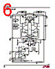
5 / 12 page  LTC3454 5 3454fa LED Power Efficiency vs LED Current Oscillator Frequency vs Temperature TEMPERATURE (°C) –55 900 920 960 980 1000 1100 1040 –15 25 45 125 3454 G16 940 1060 1080 1020 –35 5 65 85 105 VOUT = 3V VIN = 2.7V VIN = 3.6V VIN = 5.5V VIN = 4.2V ILED (mA) 100 80 85 90 900 3454 G17 75 70 60 300 500 700 200 1000 400 600 800 65 100 95 VIN = 3.6V TA = 25°C EFFICIENCY = (VOUT – VLED)ILED/VINIIN FRONT PAGE APPLICATION EN1 (Pin 1): Enable Input Pin for ISET1 Current. EN2 (Pin 2): Enable Input Pin for ISET2 Current. ISET1 (Pin 3): LED Current Programming Pin. A resistor to ground programs the current through the LED to ILED = 3850(0.8V/RISET1). This amount of current adds to any amount set by EN2/ISET2 if used. ISET2 (Pin 4): LED Current Programming Pin. A resistor to ground programs the current through the LED to ILED = 3850(0.8V/RISET2). This amount of current adds to any amount set by EN1/ISET1 if used. LED (Pin 5): Low Dropout Output for LED Current Biasing. Connect the LED between VOUT and the LED pin. SW2 (Pin 6): Switching Node. External inductor con- nects between SW1 and SW2. Recommended value is 4.7μH/5μH. VOUT (Pin 7): Buck-Boost Output Rail. Bypass to GND with a ceramic capacitor. Recommended value is 10μF. VC (Pin 8): Compensation Point for the Internal Error Amplifier Output. Connect a ceramic capacitor from VC to GND. Recommended value is 0.1μF. VIN (Pin 9): Voltage Input Supply Pin (2.7V ≤ VIN ≤ 5.5V). Bypass to GND with a ceramic capacitor. Recommended value is 10μF. SW1 (Pin 10): Switching Node. External inductor con- nects between SW1 and SW2. Recommended value is 4.7μH/5μH. Exposed Pad (Pin 11): Ground Pin. Solder to PCB ground for electrical contact and optimal thermal performance. Output Voltage Ripple Back Page Application 20mV/DIV 500ns/DIV VIN = 3.6V ILED = 500mA 3454 G19 Start-Up Transient Back Page Application 0V, 0A CH1, VOUT 1V/DIV CH2, ILED 500mA FINAL VALUE CH3, VEN1 1V/DIV 0V 5ms/DIV VIN = 3.6V ILED = 500mA 3454 G19 TYPICAL PERFORMANCE CHARACTERISTICS PIN FUNCTIONS |
|
|
Link URL |
| War ALLDATASHEET hilfreich? [ DONATE ] |
Über Alldatasheet | Werbung | Kontakt | Privatsphäre und Datenschutz | Link zum Datenblatt | Linktausch | Hersteller All Rights Reserved©Alldatasheet.com |
| Russian : Alldatasheetru.com | Korean : Alldatasheet.co.kr | Spanish : Alldatasheet.es | French : Alldatasheet.fr | Italian : Alldatasheetit.com Portuguese : Alldatasheetpt.com | Polish : Alldatasheet.pl | Vietnamese : Alldatasheet.vn Indian : Alldatasheet.in | Mexican : Alldatasheet.com.mx | British : Alldatasheet.co.uk | New Zealand : Alldatasheet.co.nz |
|
Family Site : ic2ic.com |
icmetro.com |
 German ▼
 English
 Chinese
 German
 Japanese
 Russian
 Korean
 Spanish
 French
 Italian
 Portuguese
 Polish
 Vietnamese
 Indian
 Mexican
 British
 New Zealand