|
Datenblatt-Suchmaschine für elektronische Bauteile |
|
|
Datenblatt-Suchmaschine für elektronische Bauteile |
|
STP2CMP Datenblatt(PDF) 14 Page - STMicroelectronics |
|
|
|||||||||||||||||||||||||||||
STP2CMP Datenblatt(HTML) 14 Page - STMicroelectronics |
|
|
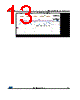
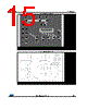
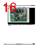
14 / 23 page  PCB layout STP2CMP 14/23 DocID022734 Rev 2 7 PCB layout 7.1 Recommended The STP2CMP is a charge pump power device so it requires a proper PCB layout in order to obtain the necessary stability and optimize line/load regulation and output voltage ripple. Input, output, and boost capacitors must be as close as possible to their relative pins.The example of the evaluation board below is shared with the STP4CMP device which is a pin compatible device with 4 current sources and the same architecture. Figure 9: Top layer |
|
|
Link URL |
| War ALLDATASHEET hilfreich? [ DONATE ] |
Über Alldatasheet | Werbung | Kontakt | Privatsphäre und Datenschutz | Link zum Datenblatt | Linktausch | Hersteller All Rights Reserved©Alldatasheet.com |
| Russian : Alldatasheetru.com | Korean : Alldatasheet.co.kr | Spanish : Alldatasheet.es | French : Alldatasheet.fr | Italian : Alldatasheetit.com Portuguese : Alldatasheetpt.com | Polish : Alldatasheet.pl | Vietnamese : Alldatasheet.vn Indian : Alldatasheet.in | Mexican : Alldatasheet.com.mx | British : Alldatasheet.co.uk | New Zealand : Alldatasheet.co.nz |
|
Family Site : ic2ic.com |
icmetro.com |
 German ▼
 English
 Chinese
 German
 Japanese
 Russian
 Korean
 Spanish
 French
 Italian
 Portuguese
 Polish
 Vietnamese
 Indian
 Mexican
 British
 New Zealand