|
Datenblatt-Suchmaschine für elektronische Bauteile |
|
|
Datenblatt-Suchmaschine für elektronische Bauteile |
|
9338 Datenblatt(PDF) 3 Page - National Semiconductor (TI) |
|
|
|
|||||||||||||||||||||||||||||
9338 Datenblatt(HTML) 3 Page - National Semiconductor (TI) |
|
|
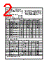
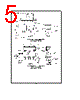
3 / 6 page  Switching Characteristics VCC ea50V TA ea25 C (See Section 1 for waveforms and load configurations) CL e 15 pF Symbol Parameter 9338 (MIL) DM9338 (COM) Units Min Max Min Max tPLH Propagation Delay 40 13 40 ns tPHL Bn or Cn to Zn 35 18 35 tPLH Propagation Delay 45 25 45 ns tPHL DA to Zn 50 25 50 tPLH Propagation Delay 35 18 35 ns tPHL CP to Zn 30 13 30 Functional Description The 9338 8-bit multiple port register can be considered a 1- bit slice of eight high speed working registers Data can be written into any one and read from any two of the eight locations simultaneously Masterslave operation eliminates all race problems associated with simultaneous readwrite activity from the same location When the clock input (CP) is LOW data applied to the data input line (DA) enters the selected master This selection is accomplished by coding the three write input select lines (A0 – A2) appropriately Data is stored synchronously with the rising edge of the clock pulse The information for each of the two slaved (output) latches is selected by two sets of read address inputs (B0 – B2 and C0 – C2) The information enters the slave while the clock is HIGH and is stored while the clock is LOW If Slave Enable is LOW (SLE) the slave latches are continuously enabled The signals are available on the output pins (ZB and ZC) The input bit selection and the two output bit selections can be accomplished independently or simultaneously The data flows into the device is demultiplexed according to the state of the write address lines and is clocked into the selected latch The eight latches function as masters and store the input data The two output latches are slaves and hold the data during the read operation The state of each slave is determined by the state of the master selected by its associ- ated set of read address inputs The method of parallel expansion is shown in Figure a One 9338 is needed for each bit of the required word length The read and write input lines should be connected in common on all of the devices This register configuration provides two words of n-bits each at one time where n devices are connected in parallel Logic Symbol TLF9794 – 2 VCC e Pin 16 GND e Pin 8 TLF9794 – 4 FIGURE a Parallel Expansion 3 |
|
|
Link URL |
| War ALLDATASHEET hilfreich? [ DONATE ] |
Über Alldatasheet | Werbung | Kontakt | Privatsphäre und Datenschutz | Link zum Datenblatt | Linktausch | Hersteller All Rights Reserved©Alldatasheet.com |
| Russian : Alldatasheetru.com | Korean : Alldatasheet.co.kr | Spanish : Alldatasheet.es | French : Alldatasheet.fr | Italian : Alldatasheetit.com Portuguese : Alldatasheetpt.com | Polish : Alldatasheet.pl | Vietnamese : Alldatasheet.vn Indian : Alldatasheet.in | Mexican : Alldatasheet.com.mx | British : Alldatasheet.co.uk | New Zealand : Alldatasheet.co.nz |
|
Family Site : ic2ic.com |
icmetro.com |
 German ▼
 English
 Chinese
 German
 Japanese
 Russian
 Korean
 Spanish
 French
 Italian
 Portuguese
 Polish
 Vietnamese
 Indian
 Mexican
 British
 New Zealand