|
Datenblatt-Suchmaschine für elektronische Bauteile |
|
|
Datenblatt-Suchmaschine für elektronische Bauteile |
|
TPD7104F Datenblatt(PDF) 3 Page - Toshiba Semiconductor |
|
|
|||||||||||||||||||||||||||||
TPD7104F Datenblatt(HTML) 3 Page - Toshiba Semiconductor |
|
|
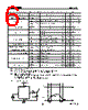
3 / 13 page  TPD7104F 2014-10-8 3 Pin Description Pin No. Symbol Function. 1 VDD Power supply pin. 2 IS Detection pin for over current. If overcurrent detection is not used, IS pin connect to GND. 3 OUT Output pin. State is off if detect overcurrent. 4 GND Ground pin. 5 GND Ground pin. 6 IN Input pin. IN has a pull-down resistor. Out is H state if VIN is H state. 7 DIAG Diagnosis detection pin. Output is inverted if detect overcurrent. 8 RISref Adjust pin for sense level for over current. If RISref is not used, RISref pin is open. Timing Chart VDD IN OUT IS VGS of outside MOSFET GND GND Normal mode Overcurrent mode Shutdown (Latch) DIAG |
|
|
Link URL |
| War ALLDATASHEET hilfreich? [ DONATE ] |
Über Alldatasheet | Werbung | Kontakt | Privatsphäre und Datenschutz | Link zum Datenblatt | Linktausch | Hersteller All Rights Reserved©Alldatasheet.com |
| Russian : Alldatasheetru.com | Korean : Alldatasheet.co.kr | Spanish : Alldatasheet.es | French : Alldatasheet.fr | Italian : Alldatasheetit.com Portuguese : Alldatasheetpt.com | Polish : Alldatasheet.pl | Vietnamese : Alldatasheet.vn Indian : Alldatasheet.in | Mexican : Alldatasheet.com.mx | British : Alldatasheet.co.uk | New Zealand : Alldatasheet.co.nz |
|
Family Site : ic2ic.com |
icmetro.com |
 German ▼
 English
 Chinese
 German
 Japanese
 Russian
 Korean
 Spanish
 French
 Italian
 Portuguese
 Polish
 Vietnamese
 Indian
 Mexican
 British
 New Zealand