|
Datenblatt-Suchmaschine für elektronische Bauteile |
|
|
Datenblatt-Suchmaschine für elektronische Bauteile |
|
AN022 Datenblatt(PDF) 3 Page - Analog Intergrations Corporation |
|
|
|||||||||||||||||||||||||||||
AN022 Datenblatt(HTML) 3 Page - Analog Intergrations Corporation |
|
|
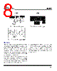
3 / 8 page  AN022 3 AIC1630A with the addition of four external switching transistors is considered as a buck converter, shown in Fig. 4. Via EXT (pin3), the internal switching of IC drives fast driving N-channel circuit, which is composed of Q1, Q2, Q3, and Q5. Bootstrapping circuit (composed of D1, D3, C5 and C7) can provide N-channel circuit with twice as much as the input voltage. When Q4 is on, the diode is used as a reverse biased. Current flows via Q4 as well as the inductor L1 to output polarity. When Q4 is off, the inductor L1 reverses its polarity with its energy transferred to the output loading, and the diode turns forward biased. Functions of the bootstrapped driver circuit and driven N-channel circuit play important roles in the application of AIC1630A and LDO with N-MOSFET circuit. 3. Bootstrapped Function As shown in Fig. 5 and 6, the peak rectifier circuit comprises two diodes (D1 and D3) and two filter capacitors (C7 and C5). And the voltage filtered by peak rectifier may provide control voltage with two times of VIN dc voltage as shown in Fig. 6 (the lower waveform). Because the output voltage is boosted up by a square waveform of amplitude VIN to two times of the input voltage, the circuit is considered as a “bootstrapped circuit”. V2 5V VPULSE V1 +5V C7 1 µF C1 470 µF D3 1N5819 D1 1N5819 10V DC + C5 100 µF Fig. 5 Bootstrapped Voltage Fig. 6 Bootstrapped Circuit Upper: D1 Cathode Polarity Signal Lower: 10VDC |
|
|
Link URL |
| War ALLDATASHEET hilfreich? [ DONATE ] |
Über Alldatasheet | Werbung | Kontakt | Privatsphäre und Datenschutz | Link zum Datenblatt | Linktausch | Hersteller All Rights Reserved©Alldatasheet.com |
| Russian : Alldatasheetru.com | Korean : Alldatasheet.co.kr | Spanish : Alldatasheet.es | French : Alldatasheet.fr | Italian : Alldatasheetit.com Portuguese : Alldatasheetpt.com | Polish : Alldatasheet.pl | Vietnamese : Alldatasheet.vn Indian : Alldatasheet.in | Mexican : Alldatasheet.com.mx | British : Alldatasheet.co.uk | New Zealand : Alldatasheet.co.nz |
|
Family Site : ic2ic.com |
icmetro.com |
 German ▼
 English
 Chinese
 German
 Japanese
 Russian
 Korean
 Spanish
 French
 Italian
 Portuguese
 Polish
 Vietnamese
 Indian
 Mexican
 British
 New Zealand