|
Datenblatt-Suchmaschine für elektronische Bauteile |
|
|
Datenblatt-Suchmaschine für elektronische Bauteile |
|
AAT4250 Datenblatt(PDF) 8 Page - Advanced Analog Technology, Inc. |
|
|
|||||||||||||||||||||||||||||
AAT4250 Datenblatt(HTML) 8 Page - Advanced Analog Technology, Inc. |
|
|
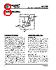
8 / 13 page  AAT4250 Slew Rate Controlled Load Switch 8 4250.2006.03.1.3 Functional Description The AAT4250 is a slew rate controlled P-channel MOSFET power switch designed for high-side load switching applications. It operates with input volt- ages ranging from 1.8V to 5.5V which, along with its extremely low operating current, makes it ideal for battery-powered applications. In cases where the input voltage drops below 1.8V, the AAT4250 MOS- FET is protected from entering the saturated region of operation by automatically shutting down. In addition, the TTL compatible ON/OFF pin makes the AAT4250 an ideal level-shifted load switch. The slew rate controlling feature eliminates inrush cur- rent when the MOSFET is turned on, allowing the AAT4250 to be used with a small input capacitor, or no input capacitor at all. During slewing, the current ramps linearly until it reaches the level required for the output load condition. The proprietary control method works by careful control and monitoring of the MOSFET gate voltage. When the device is switched ON, the gate voltage is quickly increased to the threshold level of the MOSFET. Once at this level, the current begins to slew as the gate voltage is slowly increased until the MOSFET becomes fully enhanced. Once it has reached this point, the gate is quickly increased to the full input voltage and R DS(ON) is minimized. Applications Information Input Capacitor A 1µF or larger capacitor is typically recommended for C IN in most applications. A CIN capacitor is not required for basic operation; however, it is useful in preventing load transients from affecting upstream circuits. C IN should be located as close to the device V IN pin as practically possible. Ceramic, tantalum, or aluminum electrolytic capacitors may be selected for C IN. There is no specific capacitor equivalent series resistance (ESR) requirement for C IN. However, for higher current operation, ceram- ic capacitors are recommended for C IN due to their inherent capability over tantalum capacitors to with- stand input current surges from low-impedance sources, such as batteries in portable devices. Output Capacitor For proper slew operation, a 0.1µF capacitor or greater is required between V OUT and GND. Likewise, with the output capacitor, there is no spe- cific capacitor ESR requirement. If desired, C OUT may be increased without limit to accommodate any load transient condition without adversely affecting the slew rate. Functional Block Diagram Under- Voltage Lockout Level Shift Slew Rate Control IN ON/OFF GND OUT |
|
|
Link URL |
| War ALLDATASHEET hilfreich? [ DONATE ] |
Über Alldatasheet | Werbung | Kontakt | Privatsphäre und Datenschutz | Link zum Datenblatt | Linktausch | Hersteller All Rights Reserved©Alldatasheet.com |
| Russian : Alldatasheetru.com | Korean : Alldatasheet.co.kr | Spanish : Alldatasheet.es | French : Alldatasheet.fr | Italian : Alldatasheetit.com Portuguese : Alldatasheetpt.com | Polish : Alldatasheet.pl | Vietnamese : Alldatasheet.vn Indian : Alldatasheet.in | Mexican : Alldatasheet.com.mx | British : Alldatasheet.co.uk | New Zealand : Alldatasheet.co.nz |
|
Family Site : ic2ic.com |
icmetro.com |
 German ▼
 English
 Chinese
 German
 Japanese
 Russian
 Korean
 Spanish
 French
 Italian
 Portuguese
 Polish
 Vietnamese
 Indian
 Mexican
 British
 New Zealand