|
Datenblatt-Suchmaschine für elektronische Bauteile |
|
|
Datenblatt-Suchmaschine für elektronische Bauteile |
|
AAT4250 Datenblatt(PDF) 10 Page - Advanced Analog Technology, Inc. |
|
|
|||||||||||||||||||||||||||||
AAT4250 Datenblatt(HTML) 10 Page - Advanced Analog Technology, Inc. |
|
|
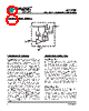
10 / 13 page  AAT4250 Slew Rate Controlled Load Switch 10 4250.2006.03.1.3 High Peak Output Current Applications Some applications require the load switch to oper- ate at a continuous nominal current level with short duration, high-current peaks. Refer to the I DM specification in the Absolute Maximum Ratings table to ensure the AAT4250’s maximum pulsed current rating is not exceeded. The duty cycle for both output current levels must be taken into account. To do so, first calculate the power dissi- pation at the nominal continuous current level, and then add the additional power dissipation due to the short duration, high-current peak scaled by the duty factor. For example, a 4V system using an AAT4250 oper- ates at a continuous 100mA load current level and has short 2A current peaks, as in a GSM applica- tion. The current peak occurs for 576µs out of a 4.61ms period. First, the current duty cycle is calculated: % Peak Duty Cycle: X/100 = 576µs/4.61ms % Peak Duty Cycle = 12.5% The load current is 100mA for 87.5% of the 4.61ms period and 2A for 12.5% of the period. Since the Electrical Characteristics do not report R DS(MAX) for 4V operation, it must be approximated by consulting the chart of R DS(ON) vs. VIN. The RDS reported for 5V R DS can be scaled by the ratio seen in the chart to derive the R DS for 4V VIN: 175mΩ x 120mΩ/115mΩ = 183m Ω. Derated for temperature: 183mΩ x (1 + 0.002800 x (125°C -25°C)) = 235m Ω. The power dissipation for a 100mA load is calculated as follows: P D(MAX) = I 2 OUT x RDS P D(100mA) = (100mA) 2 x 235m Ω P D(100mA) = 2.35mW P D(87.5%D/C) = %DC x PD(100mA) P D(87.5%D/C) = 0.875 x 2.35mW P D(87.5%D/C) = 2.1mW The power dissipation for 100mA load at 87.5% duty cycle is 2.1mW. Now the power dissipation for the remaining 12.5% of the duty cycle at 2A is cal- culated: P D(MAX) = I 2 OUT x RDS P D(2A) = (2A) 2 x 235m Ω P D(2A) = 940mW P D(12.5%D/C) = %DC x PD(2A) P D(12.5%D/C) = 0.125 x 940mW P D(12.5%D/C) = 117.5mW The power dissipation for 2A load at 12.5% duty cycle is 117mW. Finally, the two power figures are summed to determine the total true power dissipa- tion under the varied load. P D(total) = PD(100mA) + PD(2A) P D(total) = 2.1mW + 117.5mW P D(total) = 120mW The maximum power dissipation for the AAT4250 operating at an ambient temperature of 85°C is 267mW. The device in this example will have a total power dissipation of 120mW. This is well within the thermal limits for safe operation of the device; in fact, at 85°C, the AAT4250 will handle a 2A pulse for up to 28% duty cycle. At lower ambient temperatures, the duty cycle can be further increased. Printed Circuit Board Layout Recommendations For proper thermal management, and to take advantage of the low R DS(ON) of the AAT4250, a few circuit board layout rules should be followed: V IN and V OUT should be routed using wider than normal traces, and GND should be connected to a ground plane. For best performance, C IN and COUT should be placed close to the package pins. |
|
|
Link URL |
| War ALLDATASHEET hilfreich? [ DONATE ] |
Über Alldatasheet | Werbung | Kontakt | Privatsphäre und Datenschutz | Link zum Datenblatt | Linktausch | Hersteller All Rights Reserved©Alldatasheet.com |
| Russian : Alldatasheetru.com | Korean : Alldatasheet.co.kr | Spanish : Alldatasheet.es | French : Alldatasheet.fr | Italian : Alldatasheetit.com Portuguese : Alldatasheetpt.com | Polish : Alldatasheet.pl | Vietnamese : Alldatasheet.vn Indian : Alldatasheet.in | Mexican : Alldatasheet.com.mx | British : Alldatasheet.co.uk | New Zealand : Alldatasheet.co.nz |
|
Family Site : ic2ic.com |
icmetro.com |
 German ▼
 English
 Chinese
 German
 Japanese
 Russian
 Korean
 Spanish
 French
 Italian
 Portuguese
 Polish
 Vietnamese
 Indian
 Mexican
 British
 New Zealand