|
Datenblatt-Suchmaschine für elektronische Bauteile |
|
|
Datenblatt-Suchmaschine für elektronische Bauteile |
|
EV-RADAR-MMIC Datenblatt(PDF) 9 Page - Analog Devices |
|
|
|||||||||||||||||||||||||||||
EV-RADAR-MMIC Datenblatt(HTML) 9 Page - Analog Devices |
|
|
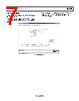
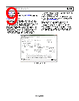
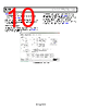
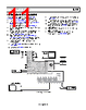
9 / 28 page  EV-RADAR-MMIC2 User Guide UG-866 Rev. B | Page 9 of 28 ADF4159 CONTROLS The ADF4159 Controls tab controls the ADF4159 device settings (see Figure 5). ADF4159 Main Controls Use the Main Controls tab to select the RF and PLL settings. In the RF Settings pane, set the RF VCO Output Frequency value to half the ADF5901 VCO output. Set the Reference Frequency value to the same frequency as the applied reference signal (TCXO or external signal) as described in the Input Signals section. The phase frequency detector (PFD) frequency is calculated from the reference frequency, the R counter, the reference doubler, and the reference divided by 2. Ensure that the PFD Frequency value matches the value specified in the loop filter design. In the PLL Settings section, program the Charge Pump Setting to the value designed for the loop. Program the Phase Detector Polarity to negative when using an inverting active loop filter configuration (use a passive loop filter on the EV-RADAR-MMIC). Select the signal that is connected to the output of the MUXOUT pin from the Muxout drop down menu. The register values are shown at the bottom of the window. When the background of a register value is green, it indicates the value changed and must be written to the device. Clicking the button below each register value writes that value to the device. Figure 5. Main Controls Tab |
|
Link URL |
| War ALLDATASHEET hilfreich? [ DONATE ] |
Über Alldatasheet | Werbung | Kontakt | Privatsphäre und Datenschutz | Link zum Datenblatt | Linktausch | Hersteller All Rights Reserved©Alldatasheet.com |
| Russian : Alldatasheetru.com | Korean : Alldatasheet.co.kr | Spanish : Alldatasheet.es | French : Alldatasheet.fr | Italian : Alldatasheetit.com Portuguese : Alldatasheetpt.com | Polish : Alldatasheet.pl | Vietnamese : Alldatasheet.vn Indian : Alldatasheet.in | Mexican : Alldatasheet.com.mx | British : Alldatasheet.co.uk | New Zealand : Alldatasheet.co.nz |
|
Family Site : ic2ic.com |
icmetro.com |
 German ▼
 English
 Chinese
 German
 Japanese
 Russian
 Korean
 Spanish
 French
 Italian
 Portuguese
 Polish
 Vietnamese
 Indian
 Mexican
 British
 New Zealand