|
Datenblatt-Suchmaschine für elektronische Bauteile |
|
|
Datenblatt-Suchmaschine für elektronische Bauteile |
|
H8SX/1663R Datenblatt(PDF) 804 Page - Renesas Technology Corp |
|
|
|||||||||||||||||||||||||||||
H8SX/1663R Datenblatt(HTML) 804 Page - Renesas Technology Corp |
|
|
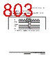
804 / 1504 page  Section 14 16-Bit Timer Pulse Unit (TPU) Rev. 2.00 Sep. 24, 2008 Page 772 of 1468 REJ09B0412-0200 14.10.10 Conflict between Buffer Register Write and Input Capture If the input capture signal is generated in the T2 state of a buffer register write cycle, the buffer operation takes precedence and the write to the buffer register is not performed. Figure 14.53 shows the timing in this case. TCNT P φ Input capture signal Address Buffer register address Write T 1 T 2 Buffer register write cycle N N TGR Buffer register M M Figure 14.53 Conflict between Buffer Register Write and Input Capture |
|
Link URL |
| War ALLDATASHEET hilfreich? [ DONATE ] |
Über Alldatasheet | Werbung | Kontakt | Privatsphäre und Datenschutz | Link zum Datenblatt | Linktausch | Hersteller All Rights Reserved©Alldatasheet.com |
| Russian : Alldatasheetru.com | Korean : Alldatasheet.co.kr | Spanish : Alldatasheet.es | French : Alldatasheet.fr | Italian : Alldatasheetit.com Portuguese : Alldatasheetpt.com | Polish : Alldatasheet.pl | Vietnamese : Alldatasheet.vn Indian : Alldatasheet.in | Mexican : Alldatasheet.com.mx | British : Alldatasheet.co.uk | New Zealand : Alldatasheet.co.nz |
|
Family Site : ic2ic.com |
icmetro.com |
 German ▼
 English
 Chinese
 German
 Japanese
 Russian
 Korean
 Spanish
 French
 Italian
 Portuguese
 Polish
 Vietnamese
 Indian
 Mexican
 British
 New Zealand