 |
Datenblatt-Suchmaschine für elektronische Bauteile |
|
|
Datenblatt-Suchmaschine für elektronische Bauteile |
|
The question interval is too short.
Please try again in a few seconds.

Hello, Please ask a question about AT25DF321A-MH-T Datasheet
# Example questions:
➢ What are the three different opcodes that can be used for the read array command, and how does the choice of opcode affect the maximum clock frequency that can be used?
➢ What happens when the device reaches the end of the memory array (3fffffh) during a read operation?
➢ Explain how the dual-output read array command differs from the standard read array command in terms of data output and pin usage.
| Part No. | AT25DF321A-MH-T |
| Manufacturer | ATMEL |
| Size | 1Mb |
| Pages | 58 pages |
| Description | 32-Megabit 2.7-volt Minimum SPI Serial Flash Memory |







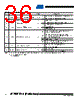
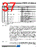






1. Overview:
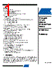
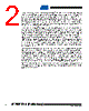
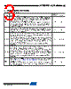
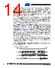
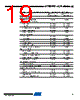
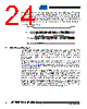
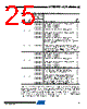
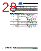
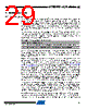
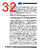
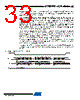
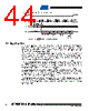
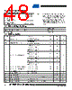
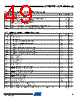
️· This document excerpt details read commands for the AT25DF321A Flash memory device. It focuses on how to read data from the device, outlining different methods and opcodes.
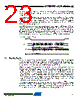
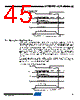
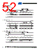
2. Read Array Command (1Bh, 0Bh, 03h Opcode):
️· Purpose: Sequential reading of data from the device.
️· Process:
- Assert CS pin.
- Clock in the appropriate opcode (1Bh, 0Bh, or 03h - choice depends on clock speed).
- Clock in the three-byte address to specify the starting location.
- Clock in a dummy byte(s) – depends on the opcode used (2 for 1Bh, 1 for 0Bh, none for 03h).
- Data streams out on the SO (Serial Output) pin, MSB (Most Significant Bit) first.
- Internal address counter auto-increments, so reading wraps around from the end of the memory array to the beginning.
️· Deasserting CS: Stops the reading.
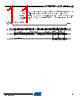
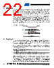
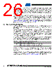
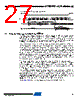
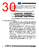
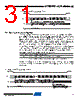
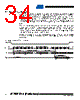
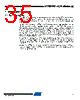
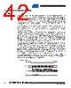
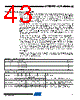
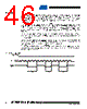
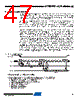
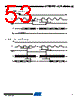
3. Dual-Output Read Array (3Bh Opcode):
️· Purpose: Similar to Read Array, but outputs *two* bits of data per clock cycle. Increases read speed.
️· Process:
- Assert CS pin.
- Clock in opcode 3Bh.
- Clock in the three-byte address.
- Clock in the dummy byte.
- Data streams out on both SO and SIO pins, MSB first. Data appears in pairs (two bits).
- Wrap around behavior is the same as the standard Read Array.
- Deasserting CS stops the process.
4. Key Considerations/Technical Details:
️· Clock Frequencies: Specific opcodes (1Bh, 0Bh, 03h, and 3Bh) are associated with different maximum clock frequencies for optimal performance. Refer to the datasheet for exact frequency limitations.
️· MSB First: Data is always output with the Most Significant Bit first.
️· Wrap-Around: The internal address counter wraps around to the beginning of the memory array after reaching the end.
️· Dummy Bytes: Required for the Read Array command.
️· SIO Pin: The second output pin used in Dual Output Read Array commands.
To fully understand this, you would need to consult the complete AT25DF321A datasheet for the precise clock frequency specifications, timing diagrams, and other relevant information.
1. Overview:
️· This document excerpt details read commands for the AT25DF321A Flash memory device. It focuses on how to read data from the device, outlining different methods and opcodes.
2. Read Array Command (1Bh, 0Bh, 03h Opcode):
️· Purpose: Sequential reading of data from the device.
️· Process:
- Assert CS pin.
- Clock in the appropriate opcode (1Bh, 0Bh, or 03h - choice depends on clock speed).
- Clock in the three-byte address to specify the starting location.
- Clock in a dummy byte(s) – depends on the opcode used (2 for 1Bh, 1 for 0Bh, none for 03h).
- Data streams out on the SO (Serial Output) pin, MSB (Most Significant Bit) first.
- Internal address counter auto-increments, so reading wraps around from the end of the memory array to the beginning.
️· Deasserting CS: Stops the reading.
3. Dual-Output Read Array (3Bh Opcode):
️· Purpose: Similar to Read Array, but outputs *two* bits of data per clock cycle. Increases read speed.
️· Process:
- Assert CS pin.
- Clock in opcode 3Bh.
- Clock in the three-byte address.
- Clock in the dummy byte.
- Data streams out on both SO and SIO pins, MSB first. Data appears in pairs (two bits).
- Wrap around behavior is the same as the standard Read Array.
- Deasserting CS stops the process.
4. Key Considerations/Technical Details:
️· Clock Frequencies: Specific opcodes (1Bh, 0Bh, 03h, and 3Bh) are associated with different maximum clock frequencies for optimal performance. Refer to the datasheet for exact frequency limitations.
️· MSB First: Data is always output with the Most Significant Bit first.
️· Wrap-Around: The internal address counter wraps around to the beginning of the memory array after reaching the end.
️· Dummy Bytes: Required for the Read Array command.
️· SIO Pin: The second output pin used in Dual Output Read Array commands.
To fully understand this, you would need to consult the complete AT25DF321A datasheet for the precise clock frequency specifications, timing diagrams, and other relevant information.
| Part No. | AT25DF321A-MH-T |
| Manufacturer | ATMEL |
| Size | 1Mb |
| Pages | 58 pages |
| Description | 32-Megabit 2.7-volt Minimum SPI Serial Flash Memory |
| War ALLDATASHEET hilfreich? [ DONATE ] |
Über Alldatasheet | Werbung | Kontakt | Privatsphäre und Datenschutz | Link zum Datenblatt | Linktausch | Hersteller All Rights Reserved©Alldatasheet.com |
| Russian : Alldatasheetru.com | Korean : Alldatasheet.co.kr | Spanish : Alldatasheet.es | French : Alldatasheet.fr | Italian : Alldatasheetit.com Portuguese : Alldatasheetpt.com | Polish : Alldatasheet.pl | Vietnamese : Alldatasheet.vn Indian : Alldatasheet.in | Mexican : Alldatasheet.com.mx | British : Alldatasheet.co.uk | New Zealand : Alldatasheet.co.nz |
|
Family Site : ic2ic.com |
icmetro.com |
 German ▼
  English
 Chinese
 Japanese
 Russian
 Korean
 Spanish
 French
 Italian
 Portuguese
 Polish
 Vietnamese
 Indian
 Mexican
 British
 New Zealand