 |
Datenblatt-Suchmaschine für elektronische Bauteile |
|
|
Datenblatt-Suchmaschine für elektronische Bauteile |
|
The question interval is too short.
Please try again in a few seconds.

Hello, Please ask a question about AT25DF321A-MH-Y Datasheet
# Example questions:
➢ What conditions will cause the write enable latch (wel) bit in the status register to be reset back to '0' during a programming operation?
➢ What must happen *before* a byte/page program command can be initiated?
➢ Explain the behavior of the device when programming data that extends beyond the end of a page boundary. what happens to the excess data?
| Part No. | AT25DF321A-MH-Y |
| Manufacturer | ATMEL |
| Size | 2Mb |
| Pages | 52 pages |
| Description | 32-Mbit 2.7V Minimum Serial Peripheral Interface Serial Flash Memory |


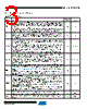


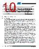
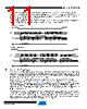
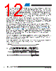

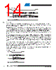


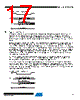
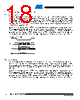
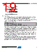


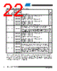
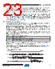
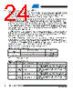
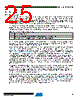

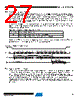
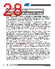
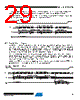
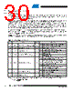
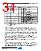
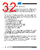
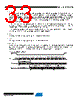
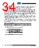


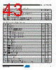
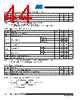
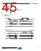
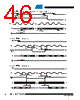



Okay, here's a summary of the key information from the provided excerpt from the Atmel AT25DF321A datasheet. I'm focusing on the most important aspects and simplifying where possible.
1. Device Overview:
️· The AT25DF321A is a memory device (likely Flash memory) with a focus on SPI (Serial Peripheral Interface) communication.
2. Read Operations:
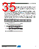
️· Read Array (1Bh Opcode): Allows sequential reading of data from the memory. Data output starts immediately after the address is sent. It wraps around from the end of the memory to the beginning.
️· Read Array (0Bh Opcode): Similar to the above but uses a different opcode.
️· Read Array (03h Opcode): Similar to the above but uses a different opcode.
️· Dual-Output Read Array (3Bh Opcode): Reads two bits of data per clock cycle, increasing data throughput.
3. Program and Erase Operations:
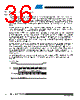
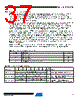
️· Byte/Page Program (02h Opcode): Programs data into memory locations.
- Requires Write Enable: A 'Write Enable' command *must* be sent first.
- Page Boundaries: If the starting address doesn't align with a page boundary, data wraps around within the page.
- Data Limit: Only the last 256 bytes of data sent are programmed.
- Programming Time: Programming is self-timed (tPP or tBP).
- Restrictions:
■ Requires a complete address and at least one byte of data.
■ CS must be deasserted on even byte boundaries.
■ Cannot program protected or locked-down sectors.
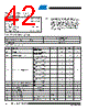
■ The WEL bit resets to 0 if the cycle aborts.
Key Considerations/Important Notes:
️· SPI Interface: This device uses SPI communication, meaning it relies on specific timing and signal protocols.
️· Write Enable Latch (WEL): Crucial for programming operations.
️· Sector Protection/Lockdown: Restrictions apply to programming within protected or locked-down sectors.
️· CS Pin Timing: Careful attention to the CS (Chip Select) pin timing is critical for successful operations.
Let me know if you would like a summary of any other sections of the datasheet!
1. Device Overview:
️· The AT25DF321A is a memory device (likely Flash memory) with a focus on SPI (Serial Peripheral Interface) communication.
2. Read Operations:
️· Read Array (1Bh Opcode): Allows sequential reading of data from the memory. Data output starts immediately after the address is sent. It wraps around from the end of the memory to the beginning.
️· Read Array (0Bh Opcode): Similar to the above but uses a different opcode.
️· Read Array (03h Opcode): Similar to the above but uses a different opcode.
️· Dual-Output Read Array (3Bh Opcode): Reads two bits of data per clock cycle, increasing data throughput.
3. Program and Erase Operations:
️· Byte/Page Program (02h Opcode): Programs data into memory locations.
- Requires Write Enable: A 'Write Enable' command *must* be sent first.
- Page Boundaries: If the starting address doesn't align with a page boundary, data wraps around within the page.
- Data Limit: Only the last 256 bytes of data sent are programmed.
- Programming Time: Programming is self-timed (tPP or tBP).
- Restrictions:
■ Requires a complete address and at least one byte of data.
■ CS must be deasserted on even byte boundaries.
■ Cannot program protected or locked-down sectors.
■ The WEL bit resets to 0 if the cycle aborts.
Key Considerations/Important Notes:
️· SPI Interface: This device uses SPI communication, meaning it relies on specific timing and signal protocols.
️· Write Enable Latch (WEL): Crucial for programming operations.
️· Sector Protection/Lockdown: Restrictions apply to programming within protected or locked-down sectors.
️· CS Pin Timing: Careful attention to the CS (Chip Select) pin timing is critical for successful operations.
| Part No. | AT25DF321A-MH-Y |
| Manufacturer | ATMEL |
| Size | 2Mb |
| Pages | 52 pages |
| Description | 32-Mbit 2.7V Minimum Serial Peripheral Interface Serial Flash Memory |
| War ALLDATASHEET hilfreich? [ DONATE ] |
Über Alldatasheet | Werbung | Kontakt | Privatsphäre und Datenschutz | Link zum Datenblatt | Linktausch | Hersteller All Rights Reserved©Alldatasheet.com |
| Russian : Alldatasheetru.com | Korean : Alldatasheet.co.kr | Spanish : Alldatasheet.es | French : Alldatasheet.fr | Italian : Alldatasheetit.com Portuguese : Alldatasheetpt.com | Polish : Alldatasheet.pl | Vietnamese : Alldatasheet.vn Indian : Alldatasheet.in | Mexican : Alldatasheet.com.mx | British : Alldatasheet.co.uk | New Zealand : Alldatasheet.co.nz |
|
Family Site : ic2ic.com |
icmetro.com |
 German ▼
  English
 Chinese
 Japanese
 Russian
 Korean
 Spanish
 French
 Italian
 Portuguese
 Polish
 Vietnamese
 Indian
 Mexican
 British
 New Zealand