|
Datenblatt-Suchmaschine für elektronische Bauteile |
|
|
Datenblatt-Suchmaschine für elektronische Bauteile |
|
AT25DF321A-MH-Y Datenblatt(PDF) 35 Page - ATMEL Corporation |
|
|
|||||||||||||||||||||||||||||
AT25DF321A-MH-Y Datenblatt(HTML) 35 Page - ATMEL Corporation |
|
|
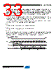
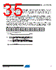
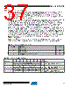
35 / 52 page  35 3686D–DFLASH–12/09 Atmel AT25DF321A 11.3 Write Status Register Byte 2 The Write Status Register Byte 2 command is used to modify the RSTE and SLE bits of the Status Register. Using the Write Status Register Byte 2 command is the only way to modify the RSTE and SLE bits in the Status Register during normal device operation, and the SLE bit can only be modified if the sector lockdown state has not been frozen. Before the Write Status Register Byte 2 command can be issued, the Write Enable command must have been previously issued to set the WEL bit in the Status Register to a logical “1”. To issue the Write Status Register Byte 2 command, the CS pin must first be asserted and the opcode of 31h must be clocked into the device followed by one byte of data. The one byte of data consists of three don’t care bits, the RSTE bit value, the SLE bit value, and three additional don’t care bits (see Table 11-4). Any additional data bytes that are sent to the device will be ignored. When the CS pin is deasserted, the RSTE and SLE bits in the Status Register will be modified, and the WEL bit in the Status Register will be reset back to a logical “0”. The SLE bit will only be modified if the Freeze Sector Lockdown State command has not been previously issued. The complete one byte of data must be clocked into the device before the CS pin is deasserted, and the CS pin must be deasserted on even byte boundaries (multiples of eight bits); otherwise, the device will abort the operation, the state of the RSTE and SLE bits will not change, and the WEL bit in the Status Register will be reset back to the logical “0” state. Figure 11-3. Write Status Register Byte 2 Table 11-4. Write Status Register Byte 2 Format Bit 7 Bit 6 Bit 5 Bit 4 Bit 3 Bit 2 Bit 1 Bit 0 X X X RSTE SLE X X X SCK CS SI SO MSB 23 1 0 0011000 67 5 4 OPCODE 10 11 9 814 15 13 12 1 MSB XXX D D X X X STATUS REGISTER IN BYTE 2 HIGH-IMPEDANCE |
|
Link URL |
| War ALLDATASHEET hilfreich? [ DONATE ] |
Über Alldatasheet | Werbung | Kontakt | Privatsphäre und Datenschutz | Link zum Datenblatt | Linktausch | Hersteller All Rights Reserved©Alldatasheet.com |
| Russian : Alldatasheetru.com | Korean : Alldatasheet.co.kr | Spanish : Alldatasheet.es | French : Alldatasheet.fr | Italian : Alldatasheetit.com Portuguese : Alldatasheetpt.com | Polish : Alldatasheet.pl | Vietnamese : Alldatasheet.vn Indian : Alldatasheet.in | Mexican : Alldatasheet.com.mx | British : Alldatasheet.co.uk | New Zealand : Alldatasheet.co.nz |
|
Family Site : ic2ic.com |
icmetro.com |
 German ▼
 English
 Chinese
 German
 Japanese
 Russian
 Korean
 Spanish
 French
 Italian
 Portuguese
 Polish
 Vietnamese
 Indian
 Mexican
 British
 New Zealand