 |
Datenblatt-Suchmaschine für elektronische Bauteile |
|
|
Datenblatt-Suchmaschine für elektronische Bauteile |
|
The question interval is too short.
Please try again in a few seconds.

Hello, Please ask a question about SST39SF010A Datasheet
# Example questions:
➢ What is the minimum data retention time specified for the sst39sf series?
➢ What are the absolute maximum ratings for voltage on any pin to ground potential?
➢ What is the difference between vih and vihc input high voltage levels, and under what conditions are they applicable?
| Part No. | SST39SF010A |
| Manufacturer | MICROCHIP |
| Size | 227 Kbytes |
| Pages | 29 pages |
| Description | 1 Mbit / 2 Mbit / 4 Mbit (x8) Multi-Purpose Flash |














1. Device Overview
️· Type: Multi-Purpose Flash Memory
️· Functionality: Designed for read-intensive and write-capable applications. Supports read, program, and erase operations.
2. Key Features & Benefits (Implied)
️· Multi-Purpose: Suitable for a wide range of applications.
️· Read-Intensive: Optimized for frequent read operations.
️· Programmable/Erasable: Allows for data storage and updates.
️· Flexible Power-Up Timings: Specifies the minimum time needed for the device to become operational after power is applied.
3. Absolute Maximum Stress Ratings & Operating Ranges
️· Temperature Range:
- *Commercial:* 0°C to +70°C
- *Industrial:* -40°C to +85°C
️· Voltage: Defined maximum voltage limits to prevent device damage.
️· Power Dissipation: Specifies the maximum power the device can handle.
️· Reliability: Describes conditions that can cause permanent damage if exceeded.
4. DC Operating Characteristics
️· Supply Current (IDD): Specifies the current drawn during various operating modes:
- *Read:* Relatively low current during read operations.
- *Program/Erase:* Higher current during program and erase cycles.
- *Standby:* Low current consumption when the device is in a standby state.
️· Input/Output Leakage Current: Limits on leakage current.
️· Voltage Levels (VIL, VIH, VOH, VOL): Defines acceptable voltage levels for input and output signals.
5. AC Characteristics (Timing)
️· Power-up timings (TPU-READ1, TPU-WRITE1): Specifies the minimum time needed for the device to become operational after power is applied.
️· Capacitance: Provides information about the capacitance of pins, which affects speed.
6. Reliability Characteristics
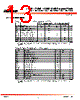
️· Endurance (NEND1,2): Specifies the number of program/erase cycles the device can reliably endure (minimum 10,000 cycles).
️· Data Retention (TDR1): Defines how long data remains stored (minimum 100 years).
️· Latch-up immunity (ILTH1): Specifies the device’s resistance to latch-up conditions.
7. Table Summary
| Table Number | Description |
|---|---|
| 5 | DC Operating Characteristics |
| 7 | AC Conditions of Test |
| 8 | Recommended System Power-up Timings |
| 9 | Capacitance |
| 10 | Reliability Characteristics |
1. Device Overview
️· Type: Multi-Purpose Flash Memory
️· Functionality: Designed for read-intensive and write-capable applications. Supports read, program, and erase operations.
2. Key Features & Benefits (Implied)
️· Multi-Purpose: Suitable for a wide range of applications.
️· Read-Intensive: Optimized for frequent read operations.
️· Programmable/Erasable: Allows for data storage and updates.
️· Flexible Power-Up Timings: Specifies the minimum time needed for the device to become operational after power is applied.
3. Absolute Maximum Stress Ratings & Operating Ranges
️· Temperature Range:
- *Commercial:* 0°C to +70°C
- *Industrial:* -40°C to +85°C
️· Voltage: Defined maximum voltage limits to prevent device damage.
️· Power Dissipation: Specifies the maximum power the device can handle.
️· Reliability: Describes conditions that can cause permanent damage if exceeded.
4. DC Operating Characteristics
️· Supply Current (IDD): Specifies the current drawn during various operating modes:
- *Read:* Relatively low current during read operations.
- *Program/Erase:* Higher current during program and erase cycles.
- *Standby:* Low current consumption when the device is in a standby state.
️· Input/Output Leakage Current: Limits on leakage current.
️· Voltage Levels (VIL, VIH, VOH, VOL): Defines acceptable voltage levels for input and output signals.
5. AC Characteristics (Timing)
️· Power-up timings (TPU-READ1, TPU-WRITE1): Specifies the minimum time needed for the device to become operational after power is applied.
️· Capacitance: Provides information about the capacitance of pins, which affects speed.
6. Reliability Characteristics
️· Endurance (NEND1,2): Specifies the number of program/erase cycles the device can reliably endure (minimum 10,000 cycles).
️· Data Retention (TDR1): Defines how long data remains stored (minimum 100 years).
️· Latch-up immunity (ILTH1): Specifies the device’s resistance to latch-up conditions.
7. Table Summary
| Table Number | Description |
|---|---|
| 5 | DC Operating Characteristics |
| 7 | AC Conditions of Test |
| 8 | Recommended System Power-up Timings |
| 9 | Capacitance |
| 10 | Reliability Characteristics |
| Part No. | SST39SF010A |
| Manufacturer | MICROCHIP |
| Size | 227 Kbytes |
| Pages | 29 pages |
| Description | 1 Mbit / 2 Mbit / 4 Mbit (x8) Multi-Purpose Flash |
| War ALLDATASHEET hilfreich? [ DONATE ] |
Über Alldatasheet | Werbung | Kontakt | Privatsphäre und Datenschutz | Link zum Datenblatt | Linktausch | Hersteller All Rights Reserved©Alldatasheet.com |
| Russian : Alldatasheetru.com | Korean : Alldatasheet.co.kr | Spanish : Alldatasheet.es | French : Alldatasheet.fr | Italian : Alldatasheetit.com Portuguese : Alldatasheetpt.com | Polish : Alldatasheet.pl | Vietnamese : Alldatasheet.vn Indian : Alldatasheet.in | Mexican : Alldatasheet.com.mx | British : Alldatasheet.co.uk | New Zealand : Alldatasheet.co.nz |
|
Family Site : ic2ic.com |
icmetro.com |
 German ▼
  English
 Chinese
 Japanese
 Russian
 Korean
 Spanish
 French
 Italian
 Portuguese
 Polish
 Vietnamese
 Indian
 Mexican
 British
 New Zealand