|
Datenblatt-Suchmaschine für elektronische Bauteile |
|
|
Datenblatt-Suchmaschine für elektronische Bauteile |
|
LTC2335-16 Datenblatt(PDF) 35 Page - Linear Technology |
|
|
|||||||||||||||||||||||||||||
LTC2335-16 Datenblatt(HTML) 35 Page - Linear Technology |
|
|
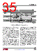
35 / 40 page  LTC2335-16 35 233516f For more information www.linear.com/LTC2335-16 applicaTions inForMaTion Figure 19. Serial LVDS I/O Mode, Direct Per-Conversion Configuration C7 C6 C5 C4 C3 C2 C1 C0 D15 D14 D13 D12 D11 D10 D9 D8 D7 D6 D5 D4 D3 D2 D1 D0 0 0 D15 CNV (CMOS) CS = PD = 0 DON’T CARE tACQ BUSY (CMOS) SCKO (LVDS) SDO (LVDS) SCKI (LVDS) SDI (LVDS) DON’T CARE DON’T CARE SAMPLE N RECOMMENDED DATA TRANSACTION WINDOW SAMPLE N + 1 CONTROL WORD FOR CONVERSION N + 1 24-BIT PACKET CONVERSION N 24-BIT PACKET CONVERSION N (REPETITION) CONVERSION RESULT CHANNEL ID SoftSpan CONVERSION RESULT 1 2 3 4 5 6 7 8 9 10 11 12 13 14 15 16 17 18 19 20 21 22 23 24 CH2 CH1 CH0 SS1 SS2 SS0 tHSDOSCKI tDSDOSCKI tBUSYLH tHSDISCKI tSCKIH tQUIET tDSDOBUSYL tCNVH tSKEW tCONV tCNVL tCYC 233516 F19 tSSDISCKI tSCKIL tSCKI program the sequencer, and outputs 24-bit packets con- tainingtheconversionresultandconfigurationinformation from the previous conversion on SDO. New data transaction windows open 10ms after power- ing up or resetting the LTC2335-16, and at the end of each conversion on the falling edge of BUSY. The data transaction should be completed with a minimum tQUIET time of 20ns prior to the start of the next conversion, as shown in Figure 19. New control words are only accepted within this recommended data transaction window, but configuration changes take effect immediately with no ad- ditional analog input settling time required before starting the next conversion. Just prior to the falling edge of BUSY and the opening of a new data transaction window, SDO is updated with the latest conversion result from the just-completed conver- sion.BothrisingandfallingedgesonSCKIseriallyclockthe conversion result and analog input channel configuration information out on SDO. SCKI is also echoed on SCKO, skew-matched to the data on SDO. Whenever possible, it is recommend that rising and falling edges of SCKO be used to capture DDR serial output data on SDO, as this will yield the best robustness to delay variations over supply and temperature. SCKI rising and falling edges also latch control words provided on SDI, which are used to set the SoftSpan range and channel for the next conversion, and program the sequencer. See the section Configuring the Multiplexer and SoftSpan Range in LVDS I/O Mode for further details. As shown in Figure 20, the LVDS bus is enabled when CS is low and is disabled and Hi-Z when CS is high, allow- ing the bus to be shared across multiple devices. Due to the high speeds often involved in LVDS signaling, LVDS bus sharing must be carefully considered. Transmission line limitations imposed by the shared bus may limit the maximum achievable bus clock speed. LVDS inputs are internallyterminatedwitha100Ωdifferentialresistorwhen CS is low, while outputs must be differentially terminated with a 100Ω resistor at the receiver (FPGA). SCKI must idle in the low state in LVDS I/O mode, including when transitioning CS. |
|
Link URL |
| War ALLDATASHEET hilfreich? [ DONATE ] |
Über Alldatasheet | Werbung | Kontakt | Privatsphäre und Datenschutz | Link zum Datenblatt | Linktausch | Hersteller All Rights Reserved©Alldatasheet.com |
| Russian : Alldatasheetru.com | Korean : Alldatasheet.co.kr | Spanish : Alldatasheet.es | French : Alldatasheet.fr | Italian : Alldatasheetit.com Portuguese : Alldatasheetpt.com | Polish : Alldatasheet.pl | Vietnamese : Alldatasheet.vn Indian : Alldatasheet.in | Mexican : Alldatasheet.com.mx | British : Alldatasheet.co.uk | New Zealand : Alldatasheet.co.nz |
|
Family Site : ic2ic.com |
icmetro.com |
 German ▼
 English
 Chinese
 German
 Japanese
 Russian
 Korean
 Spanish
 French
 Italian
 Portuguese
 Polish
 Vietnamese
 Indian
 Mexican
 British
 New Zealand