|
Datenblatt-Suchmaschine für elektronische Bauteile |
|
|
Datenblatt-Suchmaschine für elektronische Bauteile |
|
M24256E-F Datenblatt(PDF) 10 Page - STMicroelectronics |
|
|
|||||||||||||||||||||||||||||
M24256E-F Datenblatt(HTML) 10 Page - STMicroelectronics |
|
|
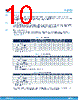
10 / 46 page  5.3 Data input During data input, the device samples serial data (SDA) on the rising edge of serial clock (SCL). For correct device operation,serial data (SDA) must be stable during the rising edge of serial clock (SCL), and the serial data (SDA) signal must change only when serial clock (SCL) is driven low. 5.4 Acknowledge bit (ACK) The acknowledge bit is used to indicate a successful byte transfer. The bus transmitter, whether it be bus master or slave device, releases serial data (SDA) after sending eight bits of data. During the 9th clock pulse period, the receiver pulls serial data (SDA) low to acknowledge the receipt of the eight data bits. 5.5 Device addressing To start communication between the bus master and the slave device, the bus master must initiate a start condition. Following this, the bus master sends the device select code and byte address as specified in Table 3, Table 4 and Table 5. Table 3. Device address Features Device type identifier Chip enable address Bit 0 (LSB) Bit 7 (MSB)(1) Bit 6 Bit 5 Bit 4 Bit 3 Bit 2 Bit 1 Memory 1 0 1 0 C2 C1 C0 R/W Identification page 1 0 1 1 C2 C1 C0 R/W Identification page lock 1 0 1 1 C2 C1 C0 R/W Configurable device address 1 0 1 1 C2 C1 C0 R/W 1. The most significant bit, b7, is sent first. Table 4. First word address Features Bit 7 (MSB)(1) Bit 6 Bit 5 Bit 4 Bit 3 Bit 2 Bit 1 Bit 0 (LSB) Memory X(2) A14 A13 A12 A11 A10 A9 A8 Identification page X(3) X(3) X(3) X X 0 X X Identification page lock X(3) X(3) X(3) X X 1 X X Configurable device address 1 1 0 X X X X X 1. The most significant bit, b7, is sent first. 2. X = Don't care 3. For identification page do not use A15/A14/A13 equal to '110' Table 5. Second word address Features Bit 7 (MSB)(1) Bit 6 Bit 5 Bit 4 Bit 3 Bit 2 Bit 1 Bit 0 (LSB) Memory A7 A6 A5 A4 A3 A2 A1 A0 Identification page X(2) X A5 A4 A3 A2 A1 A0 Identification page lock X X X X X X X X Configurable device address X X X X X X X X 1. The most significant bit, b7, is sent first. 2. X = Don't care When the device select code is received, the device responds only if the bit 3, bit 2 and bit 1 values match the values of the C2, C1 and C0 bits programmed in the configurable device address register. M24256E-F Data input DS12687 - Rev 2 page 10/46 |
|
Link URL |
| War ALLDATASHEET hilfreich? [ DONATE ] |
Über Alldatasheet | Werbung | Kontakt | Privatsphäre und Datenschutz | Link zum Datenblatt | Linktausch | Hersteller All Rights Reserved©Alldatasheet.com |
| Russian : Alldatasheetru.com | Korean : Alldatasheet.co.kr | Spanish : Alldatasheet.es | French : Alldatasheet.fr | Italian : Alldatasheetit.com Portuguese : Alldatasheetpt.com | Polish : Alldatasheet.pl | Vietnamese : Alldatasheet.vn Indian : Alldatasheet.in | Mexican : Alldatasheet.com.mx | British : Alldatasheet.co.uk | New Zealand : Alldatasheet.co.nz |
|
Family Site : ic2ic.com |
icmetro.com |
 German ▼
 English
 Chinese
 German
 Japanese
 Russian
 Korean
 Spanish
 French
 Italian
 Portuguese
 Polish
 Vietnamese
 Indian
 Mexican
 British
 New Zealand