|
Datenblatt-Suchmaschine für elektronische Bauteile |
|
|
Datenblatt-Suchmaschine für elektronische Bauteile |
|
M24256E-F Datenblatt(PDF) 4 Page - STMicroelectronics |
|
|
|||||||||||||||||||||||||||||
M24256E-F Datenblatt(HTML) 4 Page - STMicroelectronics |
|
|
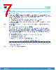
4 / 46 page  2 Signal description 2.1 Serial clock (SCL) SCL is an input. The signal applied on the SCL input is used to strobe the data available on SDA(in) and to output the data on SDA(out). 2.2 Serial data (SDA) SDA is an input/output used to transfer data in or data out of the device. SDA(out) is an open drain output that may be wire-AND with other open drain or open collector signals on the bus. A pull-up resistor must be connected from serial data (SDA) to VCC (Figure 17 and Figure 18 indicate how to calculate the value of the pull-up resistor). 2.3 Write control (WC) This input signal is useful for protecting the entire contents of the memory and the configurable device address register from inadvertent write operations. Write operations are disabled when write control (WC) is driven high. Write operations are enabled when write control (WC) is either driven low or left floating. When write control (WC) is driven high, device select and address bytes are acknowledged, data bytes are not acknowledged. 2.4 VSS (ground) VSS is the reference for the VCC supply voltage. 2.5 Supply voltage (VCC) 2.5.1 Operating supply voltage (VCC) Prior to selecting the memory and issuing instructions to it, a valid and stable VCC voltage within the specified [VCC(min), VCC(max)] range must be applied (see Operating conditions in Section 9 DC and AC parameters). In order to secure a stable DC supply voltage, it is recommended to decouple the VCC line with a suitable capacitor (from 10 nF to 100 nF) close to the VCC / VSS package pins. This voltage must remain stable and valid until the end of the transmission of the instruction and, for a write instruction, until the completion of the internal write cycle (tW). 2.5.2 Power-up conditions The VCC voltage has to rise continuously from 0 V up to the minimum VCC operating voltage (see Table 7 in Section 9 DC and AC parameters). Once the VCC is greater than, or equal to, the minimum VCC level, the master must wait for at least TWU before sending the first command to the device. See Table 13 for the value of the wake-up time parameter. 2.5.3 Device reset In order to prevent inadvertent write operations during power-up, a power-on-reset (POR) circuit is included. At power-up, the device does not respond to any instruction until VCC has reached the internal reset threshold voltage. This threshold is lower than the minimum VCC operating voltage (see Operating conditions in Section 9 DC and AC parameters). When VCC passes over the POR threshold, the device is reset and enters the Standby Power mode; however, the device must not be accessed until VCC reaches a valid and stable DC voltage within the specified [VCC(min), VCC(max)] range (see Operating conditions in Section 9 DC and AC parameters). In a similar way, during power-down (continuous decrease in VCC), the device must not be accessed when VCC drops below VCC(min). When VCC drops below the power-on-reset threshold voltage, the device stops responding to any instruction sent to it. M24256E-F Signal description DS12687 - Rev 2 page 4/46 |
|
Link URL |
| War ALLDATASHEET hilfreich? [ DONATE ] |
Über Alldatasheet | Werbung | Kontakt | Privatsphäre und Datenschutz | Link zum Datenblatt | Linktausch | Hersteller All Rights Reserved©Alldatasheet.com |
| Russian : Alldatasheetru.com | Korean : Alldatasheet.co.kr | Spanish : Alldatasheet.es | French : Alldatasheet.fr | Italian : Alldatasheetit.com Portuguese : Alldatasheetpt.com | Polish : Alldatasheet.pl | Vietnamese : Alldatasheet.vn Indian : Alldatasheet.in | Mexican : Alldatasheet.com.mx | British : Alldatasheet.co.uk | New Zealand : Alldatasheet.co.nz |
|
Family Site : ic2ic.com |
icmetro.com |
 German ▼
 English
 Chinese
 German
 Japanese
 Russian
 Korean
 Spanish
 French
 Italian
 Portuguese
 Polish
 Vietnamese
 Indian
 Mexican
 British
 New Zealand