|
Datenblatt-Suchmaschine für elektronische Bauteile |
|
|
Datenblatt-Suchmaschine für elektronische Bauteile |
|
PE42510AMLI-Z Datenblatt(PDF) 3 Page - Peregrine Semiconductor |
|
|
|||||||||||||||||||||||||||||
PE42510AMLI-Z Datenblatt(HTML) 3 Page - Peregrine Semiconductor |
|
|
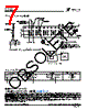
3 / 7 page  Product Specification PE42510A Page 3 of 7 Document No. 70-0266-03 │ www.psemi.com ©2008-2012 Peregrine Semiconductor Corp. All rights reserved. Evaluation Kit The PE42510A Evaluation Kit board was designed to ease customer evaluation of the PE42510A RF switch. DC power is supplied through J10, with VDD on pin 9, and GND on the entire lower row of even numbered pins. To evaluate a switch path, add or remove jumpers on CTRL/V1 (pin 3) using Table 5 (adding a jumper pulls the CMOS control pin low and removing it allows the on-board pull-up resistor to set the CMOS control pin high). J10 pins 1, 11, and 13 are N/C. The RF common port (RFC) is connected through a 50Ω transmission line via the top SMA connector, J1. RF1 and RF2 paths are also connected through 50 Ω transmission lines via SMA connectors. A 50 Ω through transmission line is available via SMA connectors J8 and J9. This transmission line can be used to estimate the loss of the PCB over the environmental conditions being evaluated. An open- ended 50 Ω transmission line is also provided at J7 for calibration if needed. Figure 4. Evaluation Board Layouts Figure 5. Evaluation Board Schematic 102-0383-02 101-0314-02 |
|
|
Link URL |
| War ALLDATASHEET hilfreich? [ DONATE ] |
Über Alldatasheet | Werbung | Kontakt | Privatsphäre und Datenschutz | Link zum Datenblatt | Linktausch | Hersteller All Rights Reserved©Alldatasheet.com |
| Russian : Alldatasheetru.com | Korean : Alldatasheet.co.kr | Spanish : Alldatasheet.es | French : Alldatasheet.fr | Italian : Alldatasheetit.com Portuguese : Alldatasheetpt.com | Polish : Alldatasheet.pl | Vietnamese : Alldatasheet.vn Indian : Alldatasheet.in | Mexican : Alldatasheet.com.mx | British : Alldatasheet.co.uk | New Zealand : Alldatasheet.co.nz |
|
Family Site : ic2ic.com |
icmetro.com |
 German ▼
 English
 Chinese
 German
 Japanese
 Russian
 Korean
 Spanish
 French
 Italian
 Portuguese
 Polish
 Vietnamese
 Indian
 Mexican
 British
 New Zealand