 |
Datenblatt-Suchmaschine für elektronische Bauteile |
|
|
Datenblatt-Suchmaschine für elektronische Bauteile |
|
The question interval is too short.
Please try again in a few seconds.

Hello, Please ask a question about AX88658AB Datasheet
# Example questions:
➢ The document details several 'nc' (no connect) pins. what is the purpose of identifying these pins in a datasheet?
➢ Describe the function of the 'f1' and 'f2' inputs, and what external components are required for proper operation of these pins?
➢ What voltage levels are required for vdd33, vdd18, and avdd18?
| Part No. | AX88658AB |
| Manufacturer | ASIX |
| Size | 328 Kbytes |
| Pages | 36 pages |
| Description | 8-Port 10/100/1000BASE-T Ethernet Switch |


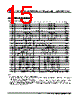

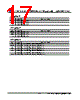


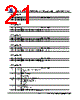


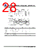


Okay, let's break down the information provided in the document. This appears to be a pinout and functional description for the AX88658AB Ethernet Switch/PHY chip.
1. Interface Ports:
️· RGMII/GMII/MII Interface Ports 0-7:
- The document details pin assignments and descriptions for 8 RGMII/GMII/MII interfaces. These ports are used to connect the chip to Ethernet MACs and transceivers.
- Key pins included: `CLK`, `RXD`, `TXD`, `RX_CTL`, `TX_CTL`, `COL`, `CRS`, `MDIO`, `MDC`, `SDIO`, `SDC`.
- Each interface has its own unique set of pins.
2. Miscellaneous Pins:
️· Power & Ground: Several pins are dedicated to power supply and ground connections. Important voltages are 3.3V, 1.8V, and specific ground planes. `VDD33`, `VDD18`, `AVDD18` are power pins, and `VSS` is ground.
️· Reset: `/RST` - Active-low reset signal.
️· Clock and Oscillator:
- `USE_8051_EN` - Enables an 8051.
- `CLK_80IN` - System clock input (85-90 MHz).
- `X_IN` - Crystal or OSC 25 MHz input for the internal PLL.
- `X_OUT` - Crystal 25 MHz output.
- `F1` & `F2`: Frequency inputs and control for PLL operation.
️· Management & EEPROM:
- `MDIO` & `MDC`: For PHY management.
- `SDIO` & `SDC`: For EEPROM communication.
️· Switch ID: `SID[4:0]` - for identifying the switch and PHYs.
️· GPIO: General Purpose Input/Output pins.
3. Key Takeaways/Important Notes:
️· External Components: Several pins (MDIO, MDC, SDIO, SDC) require external pull-up resistors. Power supplies need to be within specified tolerances.
️· PLL Operation: The PLL (Phase-Locked Loop) generates internal clocks from the `X_IN` input. The `F1` and `F2` pins are involved in this process.
️· Flexibility: The chip supports multiple interface modes (RGMII, GMII, MII) allowing for varied system designs.
If you have more questions about specific aspects of this document, or want clarification on a particular pin, just ask!
1. Interface Ports:
️· RGMII/GMII/MII Interface Ports 0-7:
- The document details pin assignments and descriptions for 8 RGMII/GMII/MII interfaces. These ports are used to connect the chip to Ethernet MACs and transceivers.
- Key pins included: `CLK`, `RXD`, `TXD`, `RX_CTL`, `TX_CTL`, `COL`, `CRS`, `MDIO`, `MDC`, `SDIO`, `SDC`.
- Each interface has its own unique set of pins.
2. Miscellaneous Pins:
️· Power & Ground: Several pins are dedicated to power supply and ground connections. Important voltages are 3.3V, 1.8V, and specific ground planes. `VDD33`, `VDD18`, `AVDD18` are power pins, and `VSS` is ground.
️· Reset: `/RST` - Active-low reset signal.
️· Clock and Oscillator:
- `USE_8051_EN` - Enables an 8051.
- `CLK_80IN` - System clock input (85-90 MHz).
- `X_IN` - Crystal or OSC 25 MHz input for the internal PLL.
- `X_OUT` - Crystal 25 MHz output.
- `F1` & `F2`: Frequency inputs and control for PLL operation.
️· Management & EEPROM:
- `MDIO` & `MDC`: For PHY management.
- `SDIO` & `SDC`: For EEPROM communication.
️· Switch ID: `SID[4:0]` - for identifying the switch and PHYs.
️· GPIO: General Purpose Input/Output pins.
3. Key Takeaways/Important Notes:
️· External Components: Several pins (MDIO, MDC, SDIO, SDC) require external pull-up resistors. Power supplies need to be within specified tolerances.
️· PLL Operation: The PLL (Phase-Locked Loop) generates internal clocks from the `X_IN` input. The `F1` and `F2` pins are involved in this process.
️· Flexibility: The chip supports multiple interface modes (RGMII, GMII, MII) allowing for varied system designs.
| Part No. | AX88658AB |
| Manufacturer | ASIX |
| Size | 328 Kbytes |
| Pages | 36 pages |
| Description | 8-Port 10/100/1000BASE-T Ethernet Switch |
| War ALLDATASHEET hilfreich? [ DONATE ] |
Über Alldatasheet | Werbung | Kontakt | Privatsphäre und Datenschutz | Link zum Datenblatt | Linktausch | Hersteller All Rights Reserved©Alldatasheet.com |
| Russian : Alldatasheetru.com | Korean : Alldatasheet.co.kr | Spanish : Alldatasheet.es | French : Alldatasheet.fr | Italian : Alldatasheetit.com Portuguese : Alldatasheetpt.com | Polish : Alldatasheet.pl | Vietnamese : Alldatasheet.vn Indian : Alldatasheet.in | Mexican : Alldatasheet.com.mx | British : Alldatasheet.co.uk | New Zealand : Alldatasheet.co.nz |
|
Family Site : ic2ic.com |
icmetro.com |
 German ▼
  English
 Chinese
 Japanese
 Russian
 Korean
 Spanish
 French
 Italian
 Portuguese
 Polish
 Vietnamese
 Indian
 Mexican
 British
 New Zealand