|
Datenblatt-Suchmaschine für elektronische Bauteile |
|
|
Datenblatt-Suchmaschine für elektronische Bauteile |
|
ADRF5062BCCZN-R7 Datenblatt(PDF) 1 Page - Analog Devices |
|
|
|||||||||||||||||||||||||||||
ADRF5062BCCZN-R7 Datenblatt(HTML) 1 Page - Analog Devices |
|
|
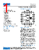
1 / 11 page  Data Sheet ADRF5062 100 MHz to 13 GHz, Differential SPDT Switch Rev. A DOCUMENT FEEDBACK TECHNICAL SUPPORT Information furnished by Analog Devices is believed to be accurate and reliable "as is". However, no responsibility is assumed by Analog Devices for its use, nor for any infringements of patents or other rights of third parties that may result from its use. Specifications subject to change without notice. No license is granted by implication or otherwise under any patent or patent rights of Analog Devices. Trademarks and registered trademarks are the property of their respective owners. FEATURES ► Frequency range: 100 MHz to 13 GHz ► Nonreflective, differential, 100 Ω impedance design ► Low insertion loss ► 0.9 dB to 10 GHz ► 1.0 dB to 13 GHz ► High isolation ► >45 dB to 10 GHz ► >40 dB to 13 GHz ► High input linearity ► P0.1dB: >34 dBm typical ► IP3: 65 dBm typical ► High power handling ► Through path: 33 dBm typical ► Terminated path: 30 dBm typical ► Hot switching: 27 dBm typical ► On and off time: 60 ns typical ► Positive control interface: CMOS-/LVTTL-compatible ► All off state control ► Pin-compatible with ADRF5063, low-frequency cutoff version ► 20-terminal, 3.0 mm × 3.0 mm LGA package APPLICATIONS ► Test instrumentation ► Data converter interfaces ► High data rate interfaces FUNCTIONAL BLOCK DIAGRAM Figure 1. Functional Block Diagram GENERAL DESCRIPTION The ADRF5062 is a silicon, nonreflective, differential, SPDT switch. The ADRF5062 operates from 100 MHz to 13 GHz with insertion loss of lower than 1.0 dB and isolation of higher than 40 dB. The ADRF5062 has a RF input power handling capability of differential 33 dBm for through paths, differential 30 dBm for terminated paths and differential 27 dBm hot switching at the RF common port. The ADRF5062 can operate with dual-supply voltages of ±3.3 V or a single-supply voltage of +3.3V when VSS is connected to GND. The ADRF5062 employs complementary metal-oxide sem- iconductor (CMOS)-compatible and low voltage transistor logic (LVTTL)-compatible controls. The ADRF5062 has an enable control to feature all off states. The ADRF5062 can also operate with a single positive supply voltage (VDD) applied while the negative supply voltage (VSS) is connected to ground. In this operating condition, the small signal performance is maintained while the switching characteristics, line- arity, and power handling performance is derated. For more details, see Table 2. The ADRF5062 is pin-compatible with the ADRF5063, low-frequen- cy cutoff version, which operates from 9 kHz to 13 GHz. The ADRF5062 comes in a 20-terminal, 3.0 mm × 3.0 mm LGA package and can operate from −40°C to +105°C. |
Ähnliche Teilenummer - ADRF5062BCCZN-R7 |
|
Ähnliche Beschreibung - ADRF5062BCCZN-R7 |
|
|
|
Link URL |
| War ALLDATASHEET hilfreich? [ DONATE ] |
Über Alldatasheet | Werbung | Kontakt | Privatsphäre und Datenschutz | Link zum Datenblatt | Linktausch | Hersteller All Rights Reserved©Alldatasheet.com |
| Russian : Alldatasheetru.com | Korean : Alldatasheet.co.kr | Spanish : Alldatasheet.es | French : Alldatasheet.fr | Italian : Alldatasheetit.com Portuguese : Alldatasheetpt.com | Polish : Alldatasheet.pl | Vietnamese : Alldatasheet.vn Indian : Alldatasheet.in | Mexican : Alldatasheet.com.mx | British : Alldatasheet.co.uk | New Zealand : Alldatasheet.co.nz |
|
Family Site : ic2ic.com |
icmetro.com |
 German ▼
 English
 Chinese
 German
 Japanese
 Russian
 Korean
 Spanish
 French
 Italian
 Portuguese
 Polish
 Vietnamese
 Indian
 Mexican
 British
 New Zealand