|
Datenblatt-Suchmaschine für elektronische Bauteile |
|
|
Datenblatt-Suchmaschine für elektronische Bauteile |
|
ADRF5062BCCZN-R7 Datenblatt(PDF) 9 Page - Analog Devices |
|
|
|||||||||||||||||||||||||||||
ADRF5062BCCZN-R7 Datenblatt(HTML) 9 Page - Analog Devices |
|
|
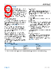
9 / 11 page  Data Sheet ADRF5062 THEORY OF OPERATION analog.com Rev. A | 9 of 11 The ADRF5062 integrates a driver to perform logic functions inter- nally and provides the user with the advantage of a simplified CMOS-/LVTTL-compatible control interface. The driver features two digital control input pins, EN and VCTL. When EN is low, the ADRF5062 is in the all off state, meaning that both RFC to RF1 and RFC to RF2 paths are in an isolation state. When EN is high, the logic level applied to the VCTL pin determines which RF port is in the insertion loss state and which RF port is in the isolation state (see Table 7). RF INPUT AND OUTPUT The RF ports (RFC, RF1, and RF2) are DC-coupled to 0 V, and no DC blocking is required at the RF ports when the RF line potential is equal to 0 V. The RF ports are internally matched to differential 100 Ω impedance. For single-ended 50 Ω applications, contact Analog Devices, Inc., Technical Support. When the EN pin is logic high, the logic level applied to the VCTL pin determines which RF port is in the insertion loss state and which RF port is in the isolation state. The insertion loss path conducts the input RF signal pair between the RFC pair and the selected RF1 and RF2 pairs. When the EN pin is logic low, the switch is in an all off state regardless of the logic state of the VCTL pin. Both the RF1 to RFC path and the RF2 to RFC path are in an isolation state. The isolation path provides high loss between the insertion loss path and the unselected RF throw pair. The unselected RF throw ports are terminated to internal differential 100 Ω resistors. The ADRF5062 is bidirectional with equal power handling capabili- ties. The RF input signal can be applied to the RFC port or to the selected RF throw port. POWER SUPPLY The ADRF5062 requires a positive supply voltage applied to the VDD pin, and a negative supply voltage applied to the VSS pin. Bypassing capacitors are recommended on the supply lines to filter high frequency noise. The ideal power-up sequence is as follows: 1. Connect GND. 2. Power up VDD and ensure that the supply is in the specified range. 3. Power up VSS. 4. Power up the digital control inputs. The relative order of the log- ic control inputs is not important. However, powering the digital control inputs before the VDD supply can inadvertently forward bias and damage the internal ESD protection structures. 5. Apply signals to the RF input port. The design is bidirectional; the input signal can be applied to the RFC port, while the RF throw ports are outputs or vice versa. The ideal power-down sequence is the reverse of the previous ideal power-up sequence. Single-Supply Operation The ADRF5062 can operate with a single positive supply voltage applied to the VDD pin, and the VSS pin connected to ground. However, some performance differences can occur in the input compression, input third-order intercept, and timing specifications. See Table 2 for further details. Table 7. Control Voltage Truth Table Digital Control Inputs RF Paths1 EN VCTL RFC to RF1 RFC to RF2 High Low Isolation (off) Insertion loss (on) High High Insertion loss (on) Isolation (off) Low Low or high Isolation (off) Isolation (off) 1 RFC refers to the RFCP and RFCN differential pair, RF1 refers to the RF1P and RF1N differential pair, and RF2 refers to the RF2P and RF2N differential pair. |
|
|
Link URL |
| War ALLDATASHEET hilfreich? [ DONATE ] |
Über Alldatasheet | Werbung | Kontakt | Privatsphäre und Datenschutz | Link zum Datenblatt | Linktausch | Hersteller All Rights Reserved©Alldatasheet.com |
| Russian : Alldatasheetru.com | Korean : Alldatasheet.co.kr | Spanish : Alldatasheet.es | French : Alldatasheet.fr | Italian : Alldatasheetit.com Portuguese : Alldatasheetpt.com | Polish : Alldatasheet.pl | Vietnamese : Alldatasheet.vn Indian : Alldatasheet.in | Mexican : Alldatasheet.com.mx | British : Alldatasheet.co.uk | New Zealand : Alldatasheet.co.nz |
|
Family Site : ic2ic.com |
icmetro.com |
 German ▼
 English
 Chinese
 German
 Japanese
 Russian
 Korean
 Spanish
 French
 Italian
 Portuguese
 Polish
 Vietnamese
 Indian
 Mexican
 British
 New Zealand