|
Datenblatt-Suchmaschine für elektronische Bauteile |
|
|
Datenblatt-Suchmaschine für elektronische Bauteile |
|
ADRF5062BCCZN-R7 Datenblatt(PDF) 10 Page - Analog Devices |
|
|
|||||||||||||||||||||||||||||
ADRF5062BCCZN-R7 Datenblatt(HTML) 10 Page - Analog Devices |
|
|
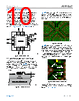
10 / 11 page  Data Sheet ADRF5062 APPLICATIONS INFORMATION analog.com Rev. A | 10 of 11 The ADRF5062 has two power supply pins (VDD and VSS) and two control pins (VCTL and EN). Figure 17 shows the external components and connections for the supply and control pins. The VDD and VSS pins are decoupled with 100 pF multilayer ceramic capacitors. The ADRF5062 pinout allows the placement of decoupling capacitors close to the device. No other external components are needed for bias and operation, except for DC blocking capacitors on the RFCx, RF1x, and RF2x pins when the RF lines are biased at a voltage different than 0 V. For more details, see the Pin Configuration and Function Descriptions section. Figure 17. Recommended Schematic RECOMMENDATIONS FOR PCB DESIGN The RF ports are matched to 50 Ω internally, and the pinout is designed to mate a coplanar waveguide (CPWG) with a 50 Ω char- acteristic impedance on the PCB. Figure 18 shows the referenced CPWG RF trace design for an RF substrate with 8 mil thick Rogers RO4003 dielectric material. The RF trace with a 14 mil width and a 7 mil clearance is recommended for 1.5 mil finished copper thickness. Figure 18. Example PCB Stack-Up Figure 19 shows the routing of the RF traces, supply, and control signals from the ADRF5062. The ground planes are connected with as many filled through vias as allowed for optimal RF and thermal performance. The primary thermal path for the ADRF5062 is the bottom side. Figure 19. PCB Routings Figure 20 shows the recommended layout from the RF pins of the ADRF5062 to the 50 Ω CPWG on the referenced stack-up. PCB pads are drawn 1:1 to the device pads. The ground pads are drawn solder mask defined, and the signal pads are drawn as pad defined. The RF trace from the PCB pad is extended with the same width till the package edge and tapered to the RF trace with a 45° angle. The paste mask is also designed to match the pad without any aperture reduction. The paste is divided into multiple openings for the paddle. Figure 20. Recommended RF Pin Transitions For alternate PCB stack-ups with different dielectric thickness and CPWG design and for further recommendations, contact Analog Devices, Inc., Technical Support. |
|
|
Link URL |
| War ALLDATASHEET hilfreich? [ DONATE ] |
Über Alldatasheet | Werbung | Kontakt | Privatsphäre und Datenschutz | Link zum Datenblatt | Linktausch | Hersteller All Rights Reserved©Alldatasheet.com |
| Russian : Alldatasheetru.com | Korean : Alldatasheet.co.kr | Spanish : Alldatasheet.es | French : Alldatasheet.fr | Italian : Alldatasheetit.com Portuguese : Alldatasheetpt.com | Polish : Alldatasheet.pl | Vietnamese : Alldatasheet.vn Indian : Alldatasheet.in | Mexican : Alldatasheet.com.mx | British : Alldatasheet.co.uk | New Zealand : Alldatasheet.co.nz |
|
Family Site : ic2ic.com |
icmetro.com |
 German ▼
 English
 Chinese
 German
 Japanese
 Russian
 Korean
 Spanish
 French
 Italian
 Portuguese
 Polish
 Vietnamese
 Indian
 Mexican
 British
 New Zealand