|
Datenblatt-Suchmaschine für elektronische Bauteile |
|
|
Datenblatt-Suchmaschine für elektronische Bauteile |
|
LT1680ISW Datenblatt(PDF) 6 Page - Linear Technology |
|
|
|||||||||||||||||||||||||||||
LT1680ISW Datenblatt(HTML) 6 Page - Linear Technology |
|
|
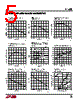
6 / 16 page  6 LT1680 TYPICAL PERFORMANCE CHARACTERISTICS RUN/SHDN Input Current vs Pin Voltage Operating Frequency (Normalized) vs Temperature Maximum Duty Cycle vs RCT RCT (kΩ) 12 4 6 100 90 80 70 60 50 40 30 20 10 0 10 20 40 60 100 1680 G20 IDISCHG = 2.1mA IDISCHG = 2.75mA FULL OPERATING TEMPERATURE RANGE TEMPERATURE ( °C) –50 1.01 1.00 0.99 0.98 25 75 1680 G21 –25 0 50 100 125 RUN/SHDN PIN VOLTAGE (V) 0 600 450 300 150 0 24 6 8 1680 G19 10 12 UPPER LIMIT LOWER LIMIT TYPICAL FULL OPERATING TEMPERATURE RANGE SL/ADJ (Pin 1): Slope Compensation Adjustment. Allows increased slope compensation for certain high duty cycle applications. Resistive loading of this pin increases effec- tive slope compensation. A resistor divider from the 5VREF pin can tailor the onset of additional slope compensation to specific regions in each switch cycle. Pin can be floated or connected to 5VREF if no additional slope compensation is required. (See Applications Information section for slope compensation details.) CT (Pin 2): Oscillator Timing Pin. Connect a capacitor (CCT) to ground and a pull-up resistor (RCT) to the 5VREF supply. Typical values are CCT = 1000pF and 10k ≤ RCT ≤ 30k. IAVG (Pin 3): Average Current Limit Integration. Fre- quency response characteristic is set using the 50k Ω output impedance and external capacitor to ground. Averaging roll-off is typically set 1 to 2 orders of magni- tude below switching frequency. (Typical capacitor value = 1000pF for fO = 100kHz.) Shorting this pin to SGND will disable the average current limit function. In systems where open-loop inductor current occurs, such as boost supplies during output short-circuit condition and inrush periods, an external small-signal protection diode should be connected between IAVG and the VC pin (anode to IAVG pin, cathode to VC pin). See Applications Information. PIN FUNCTIONS SS (Pin 4): Soft Start. Generates ramping threshold for regulator current limit during start-up and after UVLO events by sourcing about 10 µAintoanexternalcapacitor. VC (Pin 5): Error Amplifier Output. RC load creates domi- nant compensation in power supply regulation feedback loop to provide optimum transient response. (See Appli- cations Information section for compensation details.) SGND (Pin 6): Small-Signal Ground. Connect to negative terminal of COUT. VFB (Pin 7): Error Amplifier Inverting Input. Used as voltage feedback input node for regulator loop. Pin sources about 0.5 µA DC bias current to protect from an open feedback path condition. VREF (Pin 8): Bandgap Generated Voltage Reference Decoupling. Connect a capacitor to signal ground. (Typi- cal capacitor value ≈0.1µF.) SENSE + (Pin 9): Current Sense Amplifier Inverting Input. Connect to most positive (DC) terminal of current sense resistor. SENSE – (Pin 10): Current Sense Amplifier Noninverting Input. Connect to most negative (DC) terminal of current sense resistor. |
|
|
Link URL |
| War ALLDATASHEET hilfreich? [ DONATE ] |
Über Alldatasheet | Werbung | Kontakt | Privatsphäre und Datenschutz | Link zum Datenblatt | Linktausch | Hersteller All Rights Reserved©Alldatasheet.com |
| Russian : Alldatasheetru.com | Korean : Alldatasheet.co.kr | Spanish : Alldatasheet.es | French : Alldatasheet.fr | Italian : Alldatasheetit.com Portuguese : Alldatasheetpt.com | Polish : Alldatasheet.pl | Vietnamese : Alldatasheet.vn Indian : Alldatasheet.in | Mexican : Alldatasheet.com.mx | British : Alldatasheet.co.uk | New Zealand : Alldatasheet.co.nz |
|
Family Site : ic2ic.com |
icmetro.com |
 German ▼
 English
 Chinese
 German
 Japanese
 Russian
 Korean
 Spanish
 French
 Italian
 Portuguese
 Polish
 Vietnamese
 Indian
 Mexican
 British
 New Zealand