|
Datenblatt-Suchmaschine für elektronische Bauteile |
|
|
Datenblatt-Suchmaschine für elektronische Bauteile |
|
UPD161622 Datenblatt(PDF) 11 Page - NEC |
|
|
|||||||||||||||||||||||||||||
UPD161622 Datenblatt(HTML) 11 Page - NEC |
|
|
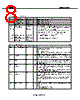
11 / 103 page  Data Sheet S15649EJ2V0DS 11 µ PD161622 3.5 Driver-Related Pins Symbol Pin Name Pad No. I/O Function S1 to S396 Source output 556 to 365, 352 to 149 Output Source output pins VCOM COM adjustment 85 Output This pin is the common adjustment output. VCOUT1 Center rectangle signal output 81, 82 Output This pin is the center rectangle signal output (Vp-p) for common modulation between 0 V to VS. VCOUT2 Center rectangle signal output 68 Output This pin is the center rectangle signal output (Vp-p) for common modulation between 0 V to VCC1. BGRIN External-power- supply connect 90 Input This is an external-power-supply connect pin for VCOM. This pin is valid when BGRS (power supply control register 1: R25) = 1. In this case, the reference voltage of the amplifier for setting the common waveform center value is input from outside the µPD161622 When BGRS = 0, power supply with built-in the µPD161622 is set up as a standard voltage for common waveform center value setup. In this case, leave it open. For more detail, refer to 5.5 Common Adjustment. VCOMR VCOM setting resistor connection 89 Input Connects an external feedback resistor for VCOM setting. This pin is valid when FBRSEL = L. In this case, connect a feedback resistor between the VCOM pin and GND. When FBRSEL = H, the amplifier for setting the common waveform center value operates as a voltage follower. In this case, leave it open. For more detail, refer to 5.5 Common Adjustment. FBRSEL VCOM setting external circuit select 92 Input This pin is used to select the method of adjusting the amplifier for setting the common waveform center value used to set the COMMON drive waveform center level. FBRSEL = H: Voltage follower circuit used (VCOMR connected to VCOM internally) FBRSEL = L: External feedback resistor used CVPH, CVPL, CVNH, CVNL Basis power supply for γ -corrected power supplies 77, 76, 75, 74 − This is operational amplifier output pin for the γ -corrected power supplies. Normally, this pin connects capacitor of 1 µF DAC0 to DAC7 D/A converter value setting 114 to 107 Input These pins set the reference voltage of the amplifier for setting the VCOM value used to set the COMMON drive waveform center level. These pins are valid when the VCOM output center value setting register (R29) = 00H and BGRS (R25: D6) = 0. This pin is pulled up to the inside IC, therefore, connect to only VSS when in low level setting pin. For more details, refer to 5.5 Common Adjustment Circuit. |
|
Link URL |
| War ALLDATASHEET hilfreich? [ DONATE ] |
Über Alldatasheet | Werbung | Kontakt | Privatsphäre und Datenschutz | Link zum Datenblatt | Linktausch | Hersteller All Rights Reserved©Alldatasheet.com |
| Russian : Alldatasheetru.com | Korean : Alldatasheet.co.kr | Spanish : Alldatasheet.es | French : Alldatasheet.fr | Italian : Alldatasheetit.com Portuguese : Alldatasheetpt.com | Polish : Alldatasheet.pl | Vietnamese : Alldatasheet.vn Indian : Alldatasheet.in | Mexican : Alldatasheet.com.mx | British : Alldatasheet.co.uk | New Zealand : Alldatasheet.co.nz |
|
Family Site : ic2ic.com |
icmetro.com |
 German ▼
 English
 Chinese
 German
 Japanese
 Russian
 Korean
 Spanish
 French
 Italian
 Portuguese
 Polish
 Vietnamese
 Indian
 Mexican
 British
 New Zealand