|
Datenblatt-Suchmaschine für elektronische Bauteile |
|
|
Datenblatt-Suchmaschine für elektronische Bauteile |
|
AX88141 Datenblatt(PDF) 12 Page - ASIX Electronics Corporation |
|
|
|||||||||||||||||||||||||||||
AX88141 Datenblatt(HTML) 12 Page - ASIX Electronics Corporation |
|
|
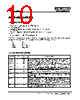
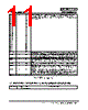
12 / 43 page  AX88141 PRELIMINARY ASIX ELECTRONICS CORPORATION 12 CONFIDENTIAL BR_A<15> BR_A<14> BR_A<13> BR_A<12> BR_A<11> BR_A<10> BR_A<9> BR_A<8> BR_A<7> BR_A<6> BR_A<5> BR_A<4> BR_A<3> BR_A<2> BR_A<1> BR_A<0> O 104, 103, 102, 101, 100, 99, 98, 97, 96, 95, 94, 93, 92, 91, 90, 89 Boot ROM address lines bit 15 to bit 0. BR_D<7> BR_D<6> BR_D<5> BR_D<4> BR_D<3> BR_D<2> BR_D<1> BR_D<0>/ SR_DO I 88, 86, 85, 84, 83, 82, 81, 73 Boot ROM data lines bit 7 to bit 0. Serial ROM data-out signal. BR_CE# O 78 Boot ROM chip enable. SR_CK O 76 Serial ROM clock signal. SR_CS O 77 Serial ROM chip-select signal. SR_DI O 79 Serial ROM data-in signal. GENP<1> GENP<0> I/O 106, 105 General-purpose pins can be used by software as either status pins or control pins. These pins can be configured by software to perform either input or output functions. Tab - 2 Boot ROM , Serial ROM , General-purpose signals group 2.4 MII interface signals group SIGNAL TYPE PIN NUMBER FOR 160 PIN DESCRIPTION COL I 113 Collision detected is asserted when detected by an external physical layer protocol(PHY) device. CRS I 114 Carrier sense is asserted by the PHY when the media is active. RXDV I 111 Data valid is asserted by an external PHY when receive data is present on the RXD lines and is deasserted at the end of the packet. This signal should be synchronized with the RXCLK signal. RXER I 109 Receive error asserts when a data decoding error is detected by an external PHY device. This signal is synchronized to RXCLK and can be asserted for a minimum of one receive clock. When asserted during a packet reception, it sets the cyclic redundancy check(CRC) error bit in the receive descriptor (RDESO). MDC O 108 MII management data clock is sourced by the AX88141 to the PHY devices as a timing reference for the transfer of information on the MII_MDIO signal. MDIO I/O 107 MII management data input/output transfers control information and status between the PHY and the AX88141. RXCLK I 115 Supports either the 25-MHZ or 2.5-MHZ receive clock. This clock is recovered by the PHY. RXD<3> RXD<2> RXD<1> RXD<0> I 119, 118, 117, 116 Four parallel receive data lines When MII mode is selected. This data is driven by an external PHY that attached the media and should be synchronized with the RXCLK signal. TXCLK I 121 Supports the 25-MHZ or 2.5-MHZ transmit clock supplied by the external physical layer medium dependent (PMD) device. This clock should always be active. TXD<3> TXD<2> TXD<1> TXD<0> O 128, 127, 125, 124 Four parallel transmit data lines. This data is synchronized to the assertion of the TXCLK signal and is latched by the external PHY on the rising edge of the TXCLK signal. TXEN O 123 Transmit enable signals that the transmit is active to an external PHY device. Tab - 3 MII interface signals group |
|
Link URL |
| War ALLDATASHEET hilfreich? [ DONATE ] |
Über Alldatasheet | Werbung | Kontakt | Privatsphäre und Datenschutz | Link zum Datenblatt | Linktausch | Hersteller All Rights Reserved©Alldatasheet.com |
| Russian : Alldatasheetru.com | Korean : Alldatasheet.co.kr | Spanish : Alldatasheet.es | French : Alldatasheet.fr | Italian : Alldatasheetit.com Portuguese : Alldatasheetpt.com | Polish : Alldatasheet.pl | Vietnamese : Alldatasheet.vn Indian : Alldatasheet.in | Mexican : Alldatasheet.com.mx | British : Alldatasheet.co.uk | New Zealand : Alldatasheet.co.nz |
|
Family Site : ic2ic.com |
icmetro.com |
 German ▼
 English
 Chinese
 German
 Japanese
 Russian
 Korean
 Spanish
 French
 Italian
 Portuguese
 Polish
 Vietnamese
 Indian
 Mexican
 British
 New Zealand