|
Datenblatt-Suchmaschine für elektronische Bauteile |
|
|
Datenblatt-Suchmaschine für elektronische Bauteile |
|
CC1010-RTY1 Datenblatt(PDF) 79 Page - Texas Instruments |
|
|
|||||||||||||||||||||||||||||
CC1010-RTY1 Datenblatt(HTML) 79 Page - Texas Instruments |
|
|
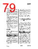
79 / 150 page  CC1010 SWRS047A Page 79 of 146 16.11 ADC The on-chip 10-bit ADC is controlled by the registers ADCON and ADCON2. Three analog pins can be sampled, selected by ADCON.ADADR. This register is also used to select the AD1 pin as external reference (when using AD0). When the AD1 pin is used as external reference, only two ADC inputs are available. The ADC output is unipolar, with an output value of 0 corresponding to 0V and 1023 corresponding to the reference voltage (1.25 V or VDD depending on the setting of the ADCREF bit). The analog reference voltage is controlled by ADCON.ADCREF. ADCON.AD_PD should be set when the ADC is not used in order to save power. A conversion can be started 5 µs after clearing the bit when using VDD or an external reference, or 100 µs afterwards when using the internal 1.25V reference. The input impedance of the ADC is a 3.2pF switched capacitor that samples the input signal once for each conversion. The average input impedance is thus: s in f C R * 1 = Average input impedances for minimum and maximum sampling frequencies are shown in Table 26. fclk fs Rin 250 kHz 22.7 kHz ~14 M Ω 32 kHz 2.9 kHz ~107 M Ω Table 26. ADC input impedance vs. sampling frequency The average input impedance accounts for the average input current to the ADC, but cannot be used for estimation of conversion errors due to voltage division between the source impedance and the ADC input impedance. For that purpose the charging time of the sample capacitor must be considered. In each conversion cycle, the input signal is sampled on the sample capacitor during one half-clock period. During this time, the accuracy of the voltage on the capacitor must reach at least ½ LSB accuracy in order to get the full accuracy of the conversion. Charging of the capacitor follows the Caharing formula: () err C f V V C t R e V e V V clk in RC t in t in ln * * 2 1 1 ln * 1 * ) 1 ( * / − = ⎟⎟ ⎠ ⎞ ⎜⎜ ⎝ ⎛ − − = ⇒ ⎟ ⎟ ⎠ ⎞ ⎜ ⎜ ⎝ ⎛ − = − = − − τ The result of this formula is the maximum output resistance of the source, for a given ADC clock frequency and accuracy. 30% safety margin should be used, due to non- perfect duty cycle etc., i.e. a maximum output resistance 30% less than calculated should be used. For ½ LSB accuracy in the charging, Table 27 shows the maximum output resistance that should be used for the source at maximum and minimum ADC clock frequencies. fclk Rmax 250 kHz 57 k Ω 32 kHz 450 k Ω Table 27. Maximum source impedance for ADC The ADC can be operated in 4 modes controlled by ADCON.ADCM. Each ADC sample conversion takes 11 ADC clock cycles. In Clock Mode 1, when X32CON.CMODE is set, the 32 kHz clock is applied directly to the ADC. The conversion time is then 344 µs. In Clock Mode 0 the ADC clock input is derived from the main oscillator clock using the divider selected by ADCON2.ADCDIV. The register must be set so that the resulting ADC clock frequency is less than or equal to 250 kHz. If the clock frequency is equal |
|
Link URL |
| War ALLDATASHEET hilfreich? [ DONATE ] |
Über Alldatasheet | Werbung | Kontakt | Privatsphäre und Datenschutz | Link zum Datenblatt | Linktausch | Hersteller All Rights Reserved©Alldatasheet.com |
| Russian : Alldatasheetru.com | Korean : Alldatasheet.co.kr | Spanish : Alldatasheet.es | French : Alldatasheet.fr | Italian : Alldatasheetit.com Portuguese : Alldatasheetpt.com | Polish : Alldatasheet.pl | Vietnamese : Alldatasheet.vn Indian : Alldatasheet.in | Mexican : Alldatasheet.com.mx | British : Alldatasheet.co.uk | New Zealand : Alldatasheet.co.nz |
|
Family Site : ic2ic.com |
icmetro.com |
 German ▼
 English
 Chinese
 German
 Japanese
 Russian
 Korean
 Spanish
 French
 Italian
 Portuguese
 Polish
 Vietnamese
 Indian
 Mexican
 British
 New Zealand