|
Datenblatt-Suchmaschine für elektronische Bauteile |
|
|
Datenblatt-Suchmaschine für elektronische Bauteile |
|
CC1010-RTY1 Datenblatt(PDF) 47 Page - Texas Instruments |
|
|
|
|||||||||||||||||||||||||||||
CC1010-RTY1 Datenblatt(HTML) 47 Page - Texas Instruments |
|
|
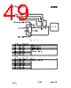
47 / 152 page  CC1010 SWRS047 Page 47 of 152 16. 8051 Peripherals CC1010 offers the following peripherals units controlled by the 8051-compatible core: • Four general-purpose I/O ports, with 26 I/O pins in total. • Two standard 8051 timers • Two timers with PWM functionality • Watchdog timer • Real-time clock • SPI master • Hardware DES encryption / decryption • Random bit generator • 10-bit ADC These modules are described in the following sections. 16.1 General Purpose I/O Four general purpose I/O-ports are available: P0, P1, P2 and P3. Table 20 shows each port and the pins on each port. Each port is associated with two registers: The port register (P0, P1, P2, or P3) and the direction register (P0DIR, P1DIR, P2DIR, or P3DIR). Each bit in the Px registers has its associated bit in the direction registers PxDIR. Setting PxDIR.y will make Px.y an input which can be read in Px(y). All pins are inputs after reset. Clearing PxDIR.y will make the pin Px.y output the data from the register Px(y). All Px and PxDIR register descriptions are shown from page 49. The structure for a single I/O-bit y on port x is shown in Figure 7. Some ports have alternate functions (such as the SPI interface), which are enabled through other registers (such as SPCR.SPE). These alternate functions may or may not override the direction setting from PxDIR as shown. When reading the Px registers, data is read from the directly from the pin. When using a read-modify-write instruction such as ANL Px, #0x01, the output register value is read and modified regardless of the setting in PxDIR. Writing to the Px registers writes to the output register, and sets the I/O pin state. Using a read-modify-write operation reads from the output register, modifies the value according to the instruction executed and writes the result back into the output register, modifying the I/O pin state accordingly. In practice, this means that the mov instruction should only be used when writing to all the pins in the port. To modify only a few pins, use a read-modify-write instruction. Also, be careful of using constructs in C or another high-level language that result in a mov from the Px registers, modify the result and write it back (without using read-modify-write instructions), as this will cause problems if not all I/O pins in the port are configured as outputs. In C, the |=, &= and ^= operators should be used to set, clear and toggle pins respectively. The CC1010 ports deviate from the standard 8051-port in the following ways: • No pull-ups / pull-downs on pins • Dedicated direction bits in PxDIR registers • CMOS output levels on all ports All general-purpose I/O pins are rated to sink or source 2 mA, except pin P2.3, which is rated to sink or source 8 mA. |
|
Link URL |
| War ALLDATASHEET hilfreich? [ DONATE ] |
Über Alldatasheet | Werbung | Kontakt | Privatsphäre und Datenschutz | Link zum Datenblatt | Linktausch | Hersteller All Rights Reserved©Alldatasheet.com |
| Russian : Alldatasheetru.com | Korean : Alldatasheet.co.kr | Spanish : Alldatasheet.es | French : Alldatasheet.fr | Italian : Alldatasheetit.com Portuguese : Alldatasheetpt.com | Polish : Alldatasheet.pl | Vietnamese : Alldatasheet.vn Indian : Alldatasheet.in | Mexican : Alldatasheet.com.mx | British : Alldatasheet.co.uk | New Zealand : Alldatasheet.co.nz |
|
Family Site : ic2ic.com |
icmetro.com |
 German ▼
 English
 Chinese
 German
 Japanese
 Russian
 Korean
 Spanish
 French
 Italian
 Portuguese
 Polish
 Vietnamese
 Indian
 Mexican
 British
 New Zealand