|
Datenblatt-Suchmaschine für elektronische Bauteile |
|
|
Datenblatt-Suchmaschine für elektronische Bauteile |
|
CC1010-RTY1 Datenblatt(PDF) 133 Page - Texas Instruments |
|
|
|
|||||||||||||||||||||||||||||
CC1010-RTY1 Datenblatt(HTML) 133 Page - Texas Instruments |
|
|
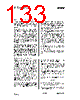
133 / 152 page  CC1010 SWRS047 Page 133 of 152 19.10 PCB Layout Recommendations Chipcon provide reference layouts that should be followed in order to achieve the best performance. The reference designs can be downloaded on the Chipcon website. A four layer PCB is highly recommended. The top layer should be used for signal routing, and the open areas should be filled with metallisation connected to ground using many vias. The second layer of the PCB should be the “ground-plane”. Layer three is used for power supply and layer four for general routing and decoupling. A few components are also placed at the reverse side (VCO inductor and power filtering). The ground pins should be connected to ground as close as possible to the package pin using individual vias for each pin. The de-coupling capacitors should also be placed as close as possible to the supply pins and connected to the ground plane by separate vias. For 868 and 915 MHz operation, some of the AVDD supply pins should be fitted with ferrite beads in series to prevent noise from coupling from one supply pin to another. Please see the reference layouts for more information. For 433 and 315 MHz operation these beads are not required, and can be replaced with 0-ohm resistors or PCB traces. The external components should be as small as possible and surface mount devices are required. The VCO inductor must be placed as close as possible to the chip and symmetrical with respect to the input pins. It is important to keep the coupling between the VCO inductor and the matching network low in order to reduce LO leakage. Due to this the VCO inductor is placed at the reverse side of the PCB. A development kit with a fully assembled PCB is available, and can be used as a guideline for layout. Full documentation and Gerber PCB layout files are available on Chipcon’s web site. 19.11 Antenna Considerations CC1010 can be used together with various types of antennas. The most common antennas for short-range devices are monopole, helical and loop antennas. Monopole antennas are resonant antennas with a length corresponding to one quarter of the electrical wavelength ( λ/4). They are very easy to design and can be implemented simply as a “piece of wire” or even integrated into the PCB. Non-resonant monopole antennas shorter than λ/4 can also be used, but at the expense of range. In size and cost critical applications such an antenna may very well be integrated into the PCB. Helical antennas can be thought of as a combination of a monopole and a loop antenna. They are a good compromise in size critical applications. But helical antennas tend to be more difficult to optimise than the simple monopole. Loop antennas are easy to integrate into the PCB, but are less effective due to difficult impedance matching because of their very low radiation resistance if they are made small. For low power applications the λ/4- monopole antenna is recommended giving the best range and because of its simplicity. The length of the λ/4-monopole antenna is given by: L = 7125 / f where f is in MHz, giving the length in cm. An antenna for 869 MHz should be 8.2 cm, and 16.4 cm for 434 MHz. The antenna should be connected as close as possible to the IC. If the antenna |
|
Link URL |
| War ALLDATASHEET hilfreich? [ DONATE ] |
Über Alldatasheet | Werbung | Kontakt | Privatsphäre und Datenschutz | Link zum Datenblatt | Linktausch | Hersteller All Rights Reserved©Alldatasheet.com |
| Russian : Alldatasheetru.com | Korean : Alldatasheet.co.kr | Spanish : Alldatasheet.es | French : Alldatasheet.fr | Italian : Alldatasheetit.com Portuguese : Alldatasheetpt.com | Polish : Alldatasheet.pl | Vietnamese : Alldatasheet.vn Indian : Alldatasheet.in | Mexican : Alldatasheet.com.mx | British : Alldatasheet.co.uk | New Zealand : Alldatasheet.co.nz |
|
Family Site : ic2ic.com |
icmetro.com |
 German ▼
 English
 Chinese
 German
 Japanese
 Russian
 Korean
 Spanish
 French
 Italian
 Portuguese
 Polish
 Vietnamese
 Indian
 Mexican
 British
 New Zealand