|
Datenblatt-Suchmaschine für elektronische Bauteile |
|
|
Datenblatt-Suchmaschine für elektronische Bauteile |
|
PIC16F570 Datenblatt(PDF) 9 Page - Microchip Technology |
|
|
|||||||||||||||||||||||||||||
PIC16F570 Datenblatt(HTML) 9 Page - Microchip Technology |
|
|
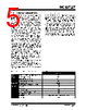
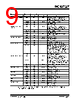
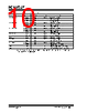
9 / 134 page  2012-2014 Microchip Technology Inc. DS40001652C-page 9 PIC16F527 TABLE 3-2: PIC16F527 PINOUT DESCRIPTION Name Function Input Type Output Type Description RA0/AN0/C1IN+/ICSPDAT RA0 TTL CMOS Bidirectional I/O pin. It can be software programmed for internal weak pull-up and wake-up from Sleep on pin change. ICSPDAT ST CMOS ICSP™ mode Schmitt Trigger. C1IN+ AN — Comparator 1 input. AN0 AN — ADC channel input. RA1/AN1/C1IN-/CVREF/ ICSPCLK RA1 TTL CMOS Bidirectional I/O pin. It can be software programmed for internal weak pull-up and wake-up from Sleep on pin change. ICSPCLK ST — ICSP™ mode Schmitt Trigger. C1IN- AN — Comparator 1 input. CVREF — AN Programmable Voltage Reference output. AN1 AN — ADC channel input. RA2/AN2/C1OUT/T0CKI RA2 TTL CMOS Bidirectional I/O port. C1OUT — CMOS Comparator 1 output. AN2 AN — ADC channel input. T0CKI ST — Timer0 Schmitt Trigger input pin. RA3/MCLR/VPP RA3 TTL — Standard TTL input with weak pull-up. MCLR ST — Master Clear (Reset). When configured as MCLR, this pin is an active-low Reset to the device. Voltage on MCLR/VPP must not exceed VDD during normal device operation or the device will enter Programming mode. Weak pull-up is always on if configured as MCLR. VPP HV — Test mode high-voltage pin. RA4/AN3/OSC2/CLKOUT RA4 TTL CMOS Bidirectional I/O pin. It can be software programmed for internal weak pull-up and wake-up from Sleep on pin change. OSC2 — XTAL Oscillator crystal output. Connections to crystal or resonator in Crystal Oscillator mode (XT, HS and LP modes only, PORTB in other modes). CLKOUT — CMOS EXTRC/INTRC CLKOUT pin (FOSC/4). AN3 AN — ADC channel input. RA5/OSC1/CLKIN RA5 TTL CMOS Bidirectional I/O port. OSC1 XTAL — XTAL oscillator input pin. CLKIN ST — EXTRC Schmitt Trigger input. RB4/OP2- RB4 TTL CMOS Bidirectional I/O port. OP2- AN — Op amp 2 inverting input. RB5/OP2+ RB5 TTL CMOS Bidirectional I/O port. OP2+ AN — Op amp 2 non-inverting input. RB6 RB6 TTL CMOS Bidirectional I/O port. RB7 RB7 TTL CMOS Bidirectional I/O port. RC0/AN4/C2IN+ RC0 ST CMOS Bidirectional I/O port. AN4 AN — ADC channel input. C2IN+ AN — Comparator 2 input. Legend: I = Input, O = Output, I/O = Input/Output, P = Power, — = Not Used, TTL = TTL input, ST = Schmitt Trigger input, HV = High Voltage, AN = Analog Voltage |
|
Link URL |
| War ALLDATASHEET hilfreich? [ DONATE ] |
Über Alldatasheet | Werbung | Kontakt | Privatsphäre und Datenschutz | Link zum Datenblatt | Linktausch | Hersteller All Rights Reserved©Alldatasheet.com |
| Russian : Alldatasheetru.com | Korean : Alldatasheet.co.kr | Spanish : Alldatasheet.es | French : Alldatasheet.fr | Italian : Alldatasheetit.com Portuguese : Alldatasheetpt.com | Polish : Alldatasheet.pl | Vietnamese : Alldatasheet.vn Indian : Alldatasheet.in | Mexican : Alldatasheet.com.mx | British : Alldatasheet.co.uk | New Zealand : Alldatasheet.co.nz |
|
Family Site : ic2ic.com |
icmetro.com |
 German ▼
 English
 Chinese
 German
 Japanese
 Russian
 Korean
 Spanish
 French
 Italian
 Portuguese
 Polish
 Vietnamese
 Indian
 Mexican
 British
 New Zealand